


20 July 2026
From road to rack: 800V EV innovations redefining AI data-center power architecture
The power electronics market for data centers will grow 2.5-fold by 2036, forecasts IDTechEx.
20 July 2026
Silicon carbide technology patent activity remained strong in Q1, says KnowMade
New patent publications in Q1/2026 exceed 460 for SiC power devices & modules and 320 for substrates & epiwafers.
20 July 2026
E-mode gallium nitride quantum well in aluminium nitride XHEMTs
The structure could also enable a combination of n-channel with p-channel HFETs for CMOS-type circuit designs.
20 July 2026
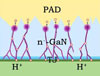
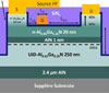
Increasing passivated AlGaN power
Researchers report a 1.7x enhancement in the Baliga figure-of-merit for a passivated AlGaN MISHEMT transistor on sapphire substrate.
20 July 2026
Purifying red InGaN micro-LED spectra
Researchers have reduced compositional pulling to achieve a single, symmetric peak in emission from red indium gallium nitride multi-quantum well micro-LEDs.
20 July 2026
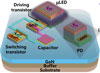
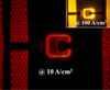
Monolithic all-GaN 2T1C-μLED–photodetector integration
Researchers at Shandong University look forward to next-generation portable and wearable intelligent terminals.
1 June 2026
Tunnel-junction micro-LEDs with 45% wall-plug efficiency
Researchers avoid post-growth thermal p-GaN activation.
1 June 2026
Nanopillar GaN LED arrays for VR and AR
Researchers fabricate 6336PPI devices with a view to future near-eye applications.

