


News: Optoelectronics
18 April 2024
III–nitride UV photonic circuits on silicon
Nanjing University of Posts and Telecommunications in China has reported on progress toward ultraviolet (UV) photonic integrated circuits (PICs) using III–nitride epitaxial layers on silicon substrates [Jiabin Yan et al, IEEE Transactions on Electron Devices, published online 2 April 2024].
The researchers integrated four diodes acting as monitor, light-emitting diode (LED), modulator, and photodetector (PD) coupled together on one level via a 50μm-wide gallium nitride waveguide (WG). The epitaxial layers of indium gallium nitride (InGaN) and aluminium gallium nitride (AlGaN) were applied by metal-organic chemical vapor deposition in a sequence typical for laser diode fabrication with waveguide and cladding layers (Figure 1).
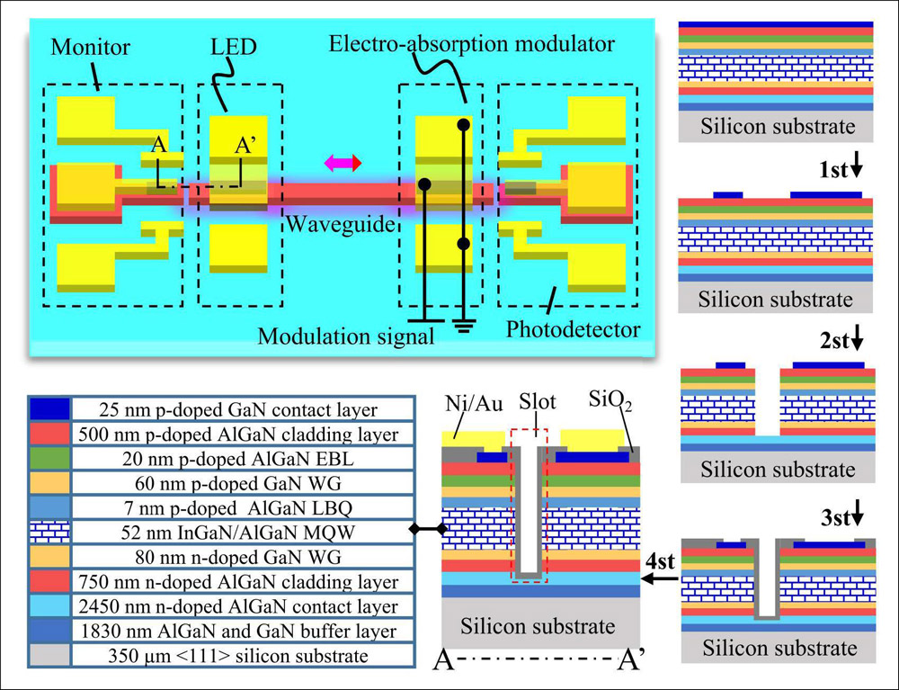
Figure 1: UV optoelectronic integrated chip scheme and associated fabrication steps.
The researchers see prospects for UV microscopy, biosensing, and on-chip data communication. The team comments: “Our integration scheme based on the epitaxial III–V on silicon is feasible for realizing a compact, low-cost, and low-complexity PIC system.”
The III–nitride layers are necessary to access and transmit UV light since silicon absorbs such radiation almost completely as UV photon energies are much higher than silicon’s bandgap energy. However, for thermal and cost considerations a silicon substrate provides higher thermal conductivity than more expensive alternatives like sapphire.
The researchers comment: “Although the data transmission rate via the modulator is currently severely limited, the PIC chip has potential prospects for audio transmission and sensor applications.”
The active layer of the structure consisted of four InGaN multiple quantum wells (MQWs) separated by AlGaN barriers. The last quantum barrier layer (LBQ) of the MQW sequence was p-doped. The epitaxial structure included an electron-blocking layer (EBL) to prevent losses from electrons overshooting the MQW and recombining non-radiatively in the hole injection layers.
The monitor and photodetector were separated from the main waveguide by slots etched down to the n-type cladding layer.
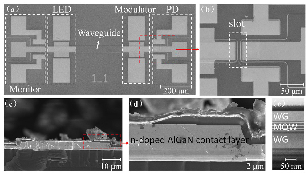
Figure 2: Scanning electron microscope (SEM) images: (a) Complete PIC. (b) Slot region between modulator and photodetector. (c) Waveguide modulator. (d) Waveguide edge. (e) Waveguide layers.
The etching for the PIC (Figure 2) used inductively coupled plasma (ICP) consisting of hydrogen chloride and boron trichloride in two steps: first to pattern the p-type contact layers, and then down to the n-cladding/contact layers to form the mesa and slot structures. Electrical isolation was provided by 100nm silicon dioxide (SiO2) applied by plasma-enhanced chemical vapor deposition. The electrode consisted of nickel/gold (Ni/Au).
Table 1: Component performance parameters.
Component |
Parameter | Value |
| LED | Output power | 0.53mW (@20mA) |
| LED | 3dB bandwidth | 64MHz |
| LED | Peak wavelength | 385nm |
| Modulator | Modulation depth | 8.4% |
| Modulator | Efficiency | 0.05dB/V |
| Modulator | 3dB bandwidth | 600Hz |
| PD | Responsivity | 112mA/W (@−6V bias) |
| PD | Detectivity | 9.3x1010cm-Hz1/2/W |
| PD | 3dB bandwidth | 33MHz |
| WG | Optical loss | 11dB/mm |
The waveguide optical loss was relatively high at 11dB/mm (Table d). The team put this down to absorption in the MQW layer and rough etched sidewalls. The researchers hope that smoother sidewalls could be achieved in the future. The narrower 3dB bandwidth of the modulation could be limited by a slow response of the electric field distribution under reverse bias voltage, the team reports.
The researchers performed a series of modulation tests on the PIC (Figure 3). The researchers suggest that direct and indirect modulation could be used simultaneously. “For example, a video signal can be transmitted using direct modulation via the LED, while a voice signal is transmitted using indirect modulation via the modulator,” the team proposes.
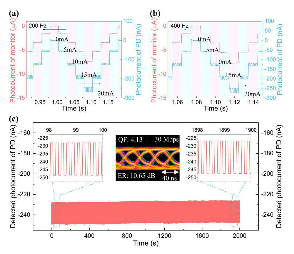
Figure 3: (a) Received photocurrent waveforms of monitor and photodetector due to multi-step current applied on LED and square signal of 200Hz frequency applied on modulator. (b) Received waveforms from multi-step current on LED and 400Hz on modulator. (c) Photodetector detection response to 5Hz modulation on modulator over 10,000 cycles. Inset: eye diagram using 30 megabits/second direct modulation on LED.
While presently direct modulation allows higher data transmission rates, it suffers from nonlinear distortion, transient heating effects, and RC delays.
The team comments on the advantages of using a modulator: “First, the design of light source and modulator can be separated and more flexibility can be obtained. Second, multiple channels via individual modulators can share a single light source, thus reducing the size of the devices and the total power budget of the system. Moreover, by using direct and indirect modulations for a single light path, two types of data can be transmitted simultaneously or one of the modulations can encrypt the data transmission of another modulation signal.”
UV photonic circuits InGaN AlGaN
https://doi.org/10.1109/TED.2024.3379151
The author Mike Cooke is a freelance technology journalist who has worked in the semiconductor and advanced technology sectors since 1997.


