


News: Microelectronics
30 April 2024
Enkris and Incize enter strategic partnership
Enkris Semiconductor of Suzhou, Jiangsu, China, a pure-play foundry for gallium nitride (GaN) epitaxial wafers, has reached a memorandum of understanding with Incize, Belgium to enter a strategic cooperation on modeling, simulation, and testing of GaN-on-Si epitaxial technology for wireless communication applications.
 Figure 1: Dr. Kai Cheng, Founder and CEO of Enkris, and Dr. Mostafa Emam, Founder and CEO of Incize, signed a memorandum of understanding on 23rd April 2024.
Enkris and Incize have been working together since 2019 to elevate the quality standards of GaN-on-Si epi wafers to meet the needs of wireless communication applications. Based on the results of that collaboration, the firms have now decided to formalize and strengthen their strategic partnership in order to push more innovative products into the market.
As epitaxial material technology has developed, GaN-on-Si wireless devices have made significant progress. However, GaN-on-Si technology entails higher losses of signal power, which limits the frequency and power characteristics of GaN HEMT-on-Si. Enkris’ Low Loss GaN on Si wafers incorporate innovative buffer optimization, which the firm says significantly improves the wireless communication performance, leading to a comparable RF loss with that of Trap-rich SOI. This, adds the firm, will pave the way for GaN-on-Si technology to become the mainstream standard for wireless infrastructure.
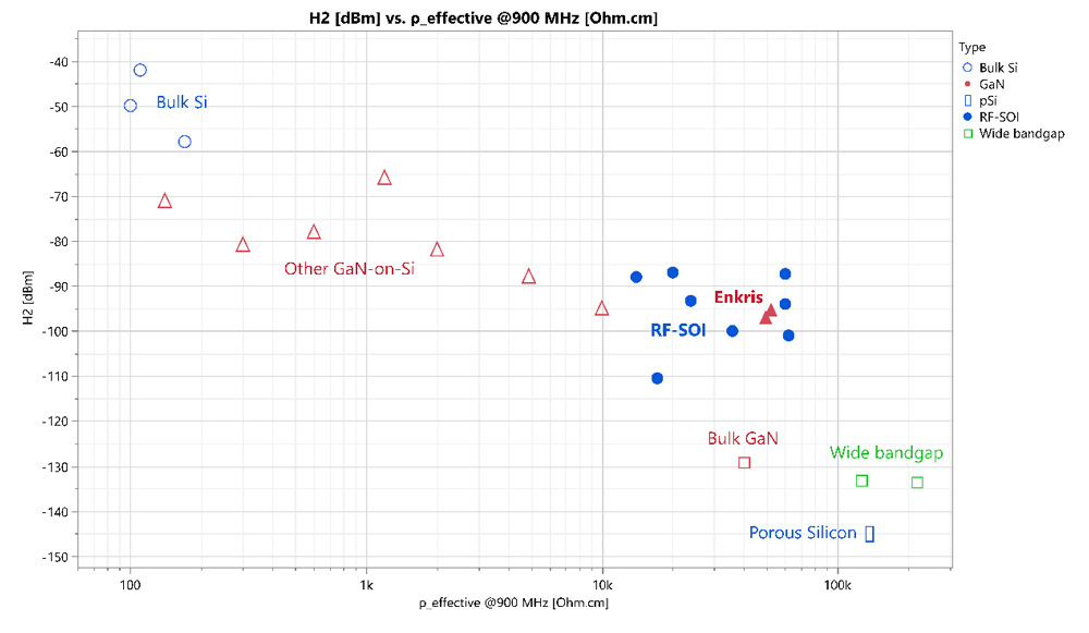
Figure 2: Benchmark plot of second harmonic distortion (more negative values are better) showing Enkris Low Loss GaN on Si (solid triangles) compared with other GaN-on-Si providers (open triangles) as well as with Trap-rich SOI technology (solid circles).
Dr. Mostafa Emam, founder and CEO of Incize, said, "Incize is a Belgian company known for innovative material testing and modeling, thanks to its industry-leading modeling, design, and testing teams, and state-of-the-art test equipment. Incize's customers include foundries, wafer manufacturers, and IC design companies. Advocating for the revitalization of the European semiconductor ecosystem, Incize also provides high-quality services to all its customers around the world. Incize strongly believes that, for front-end companies to design better wireless communication chips, it is critical to innovate and upgrade the substrates and the underlying technology and is willing to actively participate in and help the innovation efforts of wafer manufacturers, such as Enkris. Enkris has become a major player in the epi wafer manufacturing of III-V materials in a record time and has a deep culture of R&D, which aligns perfectly with our experience and service portfolio at Incize."
Dr. Kai Cheng, founder and CEO of Enkris, said, "Enkris has now made great progress in both the sales client side and the production supply chain side cum technology side in terms of GaN-on-Si epi wafers for different applications, among which the wireless communication applications, being a highly demanding and promising market. It is pleased to reinforce the already existing collaboration between Enkris and Incize and advance a step further towards a long-term collaboration that shall promote the next generation of GaN-on-Si technology, together with a new generation of wireless communication devices. Incize has advanced test equipment professional processes, and component modeling team resources. Such a partnership shall provide Enkris with the opportunity to experiment with deep innovation in materials and epi wafers".


