


News: Markets
21 June 2023
Emerging substrates market growing at 27% CAGR from $63.6m in 2022 to $264m by 2028
Due to the need to improve the performance and the cost limits, new materials, platforms and designs are continually being investigated in the semiconductor industry. In the previous decade, some compound semiconductors, such as gallium arsenide (GaAs) for radio frequency (RF) and silicon carbide (SiC) for power electronics, have succeeded in competing with silicon and have entered the mass market.
So, which emerging semiconductor substrate will be the next game changer? In its new report ‘Emerging Semiconductor Substrates 2023’, Yole Intelligence (part of Yole Group) investigates the technological status of emerging semiconductor substrates, including gallium antimonide (GaSb), indium antimonide (InSb), bulk gallium nitride (GaN), gallium oxide (Ga2O3), bulk aluminium nitride (AlN), and diamond, as well as engineered substrates and templates. Furthermore, the market research and strategy consulting company examines various potential applications such as power electronics, RF and photonics, including laser diodes, light-emitting diodes (LEDs), sensors, and detectors.
Including GaSb, InSb, bulk GaN, Ga2O3, bulk AlN, and diamond, as well as engineered substrates and templates, the emerging substrates market was valued at $63.6m in 2022 is estimated to be growing at a CAGR of 27% to more than $264.5m by 2028.
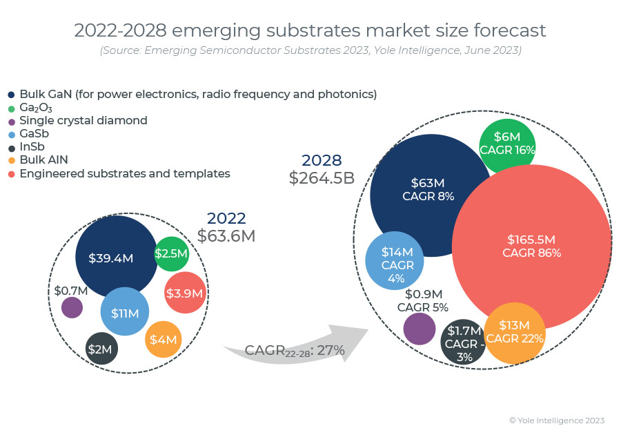
“The power electronics market, driven by several applications such as EV/HEV (electric and hybrid electric vehicles), renewable energy, and power supplies, is still dominated by silicon-based technologies,” notes Taha Ayari Ph.D., technology & market analyst, Compound Semiconductor and Emerging Substrates, at Yole Intelligence. “Nevertheless, the wide-bandgap materials SiC and GaN (lateral GaN HEMT on silicon or sapphire) have penetrated the power electronics market after a long development process and are expected to constitute more than 25% of the power electronics market by 2028,” he adds. “Benefitting from this momentum, Yole Intelligence expects bulk GaN for vertical GaN devices and engineered substrates (SmartSiC from Soitec, SiCkrest from SICOXS, and QST from Qromis) to grow in the coming five years.”
The photonics market, on the other hand, enjoys stable growth with GaSb-based devices such as infrared (IR) lasers and imagers driven mainly by high-end and niche military applications. The report also reviews the market status of InSb.
Concerning bulk GaN substrates in consumer, industrial and automotive applications, the market is considered to be stable, with a stronger push into industrial applications. During the pandemic, UVC disinfection/purification systems started using bulk AlN substrates. This could drive the AlN substrate market to a compound annual growth rate (CAGR) during 2022–2028 of 22%, the highest among all the emerging photonics substrates.
“Emerging substrate activities focus mainly on technological development for better material quality, higher yields and lower production costs,” notes Ali Jaffal Ph.D., technology & market analyst specializing in Compound Semiconductors and Emerging Substrates at Yole Intelligence. “This push needs, of course, to be supported by market demand and adoption in volume applications which defines the correct specification of the different substrates. This comes together with increasing the substrate diameter, which gives the impetus to emerging substrates industry to go towards mass production.”
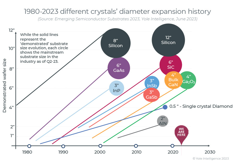
For the power electronics industry, a wafer size of at least 6-inches is needed for established foundries to be involved at high volumes. This pushes the substrate players to optimize the manufacturing techniques and to increase the wafer sizes. For diamond, the mosaic diamond method from etch pitch density (EDP) that delivers up to 28mm x 28mm and heterogeneous diamond growth on silicon or sapphire substrates from Orbray or Audiatec up to about 6-inch diameter have been developed. In addition, 6-inch bulk GaN substrates have been demonstrated using hydride vapor phase epitaxy (HVPE) and other techniques, although more work is still needed to improve the material quality and meet application requirements. Similarly, for Ga2O3, different melt growth techniques are being used, with EFG (edge-defined film-fed growth) being the most promising to obtain 6-inch wafers with acceptable material quality in volume production. Regarding engineered substrates, advanced splitting and bonding techniques are used to overcome challenges for larger single-crystal substrates and better material quality.


