


News: Optoelectronics
24 March 2022
Extending interband cascade laser wavelength
University of Oklahoma and Sandia National Laboratories in the USA have reported a record long wavelength for III-V interband cascade lasers (ICLs) of more than 13μm [J. A. Massengale et al, Appl. Phys. Lett., v120, p091105, 2022]. The research team also reports improved performance of shorter ~11μm wavelength devices in continuous wave (cw) operation. These coherent mid-infrared wavelengths find employment in gas/chemical sensing, imaging, and industrial process control.
The ICL structures were grown on indium arsenide (InAs) substrates, using molecular beam epitaxy (MBE). ICLs are frequently grown on gallium antimonide (GaSb), spanning the 3-6μm range, operating even at room temperature (300K). At present, GaSb structures suffer from the needed optical cladding becoming too thick at longer wavelengths.
The advanced waveguide structure for the Oklahoma/Sandia work consisted of 1.65μm intermediate superlattice cladding and 0.83μm InAs separate-confinement layers (SCLs).
Further optical confinement was provided by n+-InAs plasmon cladding layers — 2μm on the bottom and 1.1μm on the top. The plasmon cladding used 54% reduced doping compared with the group’s previous work with the aim of reducing optical losses from free-carrier absorption. ‘Plasmons’ refer to the quasi-particles of the quantum description of the plasma oscillations of electron charge density responsible for the typical visible light reflectivity of metals.
The light-generating 20-stage cascade structure (Figure 1) was grown with and without phosphide barrier layers. The indium arsenide phosphide (InAsP) layer insertion between an aluminium antimonide arsenide (AlSbAs) barrier and InAs electron well improved the overlap of the electron and hole wavefunctions, enhancing recombination into photons in the W-shaped ‘type-II’ well structure. The hole well consisted of gallium indium antimonide (GaInSb).
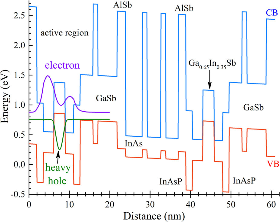
Figure 1: Band-edge diagram of one cascade stage and layer sequence for longer-wavelength ICL wafer.
The researchers comment that the InAsP barrier “can lower the electron energy level for longer-wavelength emission without increasing the InAs layer thickness.” The lower electron level reduces the energy gap with the hole energy, which should lead to lower-energy, longer-wavelength photons.
The laser material was fabricated into broad-area cavities cleaved into 1.5mm-long bars epi-side up on copper heatsinks. There was no facet coating.
The structure without InAsP barriers emitted laser light around 11μm in cw mode up to 100K, and in pulsed mode up to 130K. The InAsP lasers only operated in pulsed mode up to 120K, but the 13μm wavelength was the longest reported so far for III-V interband lasers.
The cw performance of the ICL without InAsP barrier layers had a 23A/cm2 threshold at 80K, about four times smaller than the group’s previous 20-stage ICL. However, the threshold voltage was more than 2x higher at 9.2V. “The abnormally high Vth could be caused by a possible problem in the carrier transport, which is not understood at this moment,” the team comments. These problems limited the temperature range of the devices.
The maximum cw output power of 14.3mW/facet at 80K with 172mA injection was around 4x that of the group’s previous work. The wavelength was 10.2μm. In pulsed operation, the wavelength increased to 10.85μm at 137K.
The longer-wavelength material had wavelengths under pulsed operation varying from 12.7μm at 80K to 13.23μm at 115K. The 80K pulsed mode threshold was 179A/cm2 for the current density, and 7.5V for voltage. These thresholds naturally increased at higher temperature.
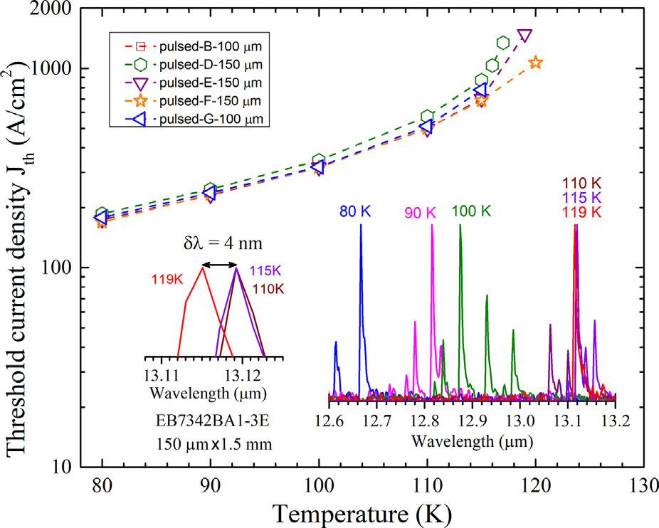
Figure 2: Threshold current density as function of temperature for several 100μm- and 150μm-width devices from wafer with InAsP barrier. Right inset: pulsed lasing spectra; left inset: zoomed-in view of blue-shift between 110-119K.
Other devices from the same wafer were able to operate beyond 115K, up to 120K, but with slightly shorter wavelengths (Figure 2). The reduction in wavelength was blamed on band-filling effects: “As lasing emission is pushed toward longer wavelengths with increasing temperature, the waveguide loss rapidly increases and there also tends to be a reduced modal overlap with the gain medium.”
III-V interband cascade lasers ICLs InAs substrates MBE GaSb InAsP AlSbAs
https://doi.org/10.1063/5.0084565
The author Mike Cooke is a freelance technology journalist who has worked in the semiconductor and advanced technology sectors since 1997.


