


News: Optoelectronics
9 March 2022
Ranovus delivers first monolithic 100G optical I/O cores for data centers based on GF Fotonix platform
At the Optical Fiber Communications conference (OFC 2022) in San Diego, CA, USA (8-10 March), Ranovus Inc of Ottawa, Ontario, Canada (which develops and manufactures multi-terabit photonics interconnect solutions for data-center and communications networks) has announced the availability of its protocol-agnostic Odin 100G optical I/O cores based on GF Fotonix, the new next-generation monolithic platform of US-based GlobalFoundries. GF Fotonix is reckoned to be first in the industry to combine 300mm photonics and RF-CMOS features on a silicon wafer, delivering what is claimed to be best-in-class performance at scale.
Odin 100G optical I/O chiplets and IP cores can be integrated with processors, switches and memory appliances to enable new data-center architectures for machine learning (ML), artificial intelligence (AI), metaverse, cloud, 5G communications, and defence and aerospace workloads. Data centers are increasingly demanding efficient and cost-effective high-capacity interconnect solutions to meet the exponential growth in data-driven applications like ML/AI and metaverse. Odin 100Gbps optical I/O scales from 8- to 32-cores in the same footprint by combining Ranovus’ 100Gbps-per-wavelength monolithic EPIC (electro-photonic integrated circuit) cores with its proprietary laser and advanced packaging technologies.
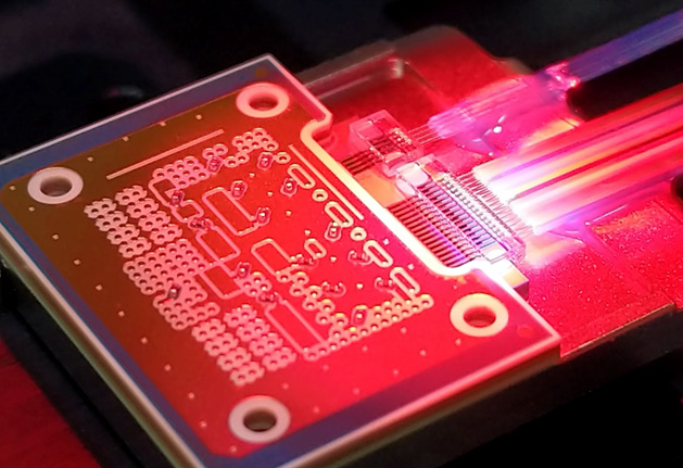
Picture: An 8-core Ranovus Odin 100Gbps optical I/O with internal and external laser source options for high-capacity data-center interconnect.
“We are delighted to share our multi-disciplinary silicon photonics IP cores and chiplets, and advanced packaging solutions with our customers who are driving the adoption of novel data-center architectures based on integrating best-in-class chiplets and co-packaged optics,” says chief business development officer Hojjat Salemi. “Our close collaboration with GlobalFoundries underlines our joint commitment to deliver a fully featured set of qualified IP cores and chiplets with OSAT-ready high-volume manufacturing flows and supporting ecosystem to enable the huge potential of monolithic silicon photonics.”
Ranovus has developed a highly flexible co-packaged optics architecture (Analog-Drive CPO 2.0) together with a tier-1 ecosystem for high-volume manufacturing of Odin chiplets. The first customer co-packaged solution with 800Gbps Odin optical I/O is also being demonstrated at OFC, with samples based on the GF Fotonix platform shipping now.
“Data centers, computing and sensing applications require incredible processing, transmission and power efficiency as the world’s data needs soar dramatically,” comments Anthony Yu, vice president, Computing and Wired Infrastructure strategic business unit at GF. “Ranovus’ IP cores, chiplets and advanced packaging solutions, combined with GF Fotonix, provide customers a complete solution to develop the chips needed solve some of the biggest challenges facing data centers today.”
At OFC, Ranovus is exhibiting in booth 5917 and GlobalFoundries in booth 4604.


