


News: Suppliers
19 January 2022
EVG launches automated SmartNIL nanoimprint and wafer-level optics system
EV Group of St Florian, Austria – a supplier of wafer bonding and lithography equipment for semiconductor, micro-electro-mechanical systems (MEMS) and nanotechnology applications – has introduced the EVG7300 automated SmartNIL nanoimprint and wafer-level optics system as its most advanced solution, combining multiple UV-based process capabilities such as nanoimprint lithography (NIL), lens molding and lens stacking (UV bonding), in a single platform.
The industry-ready, multi-functional system is designed to serve advanced R&D and production needs for a wide range of emerging applications involving micro- and nano-patterning as well as functional layer stacking. These include wafer-level optics (WLO), optical sensors and projectors, automotive lighting, waveguides for augmented reality (AR) headsets, bio-medical devices, meta-lenses and meta-surfaces, and optoelectronics. Supporting wafer sizes up to 300mm and featuring high-precision alignment, advanced process control and high throughput, the EVG7300 meets the high-volume manufacturing needs for a variety of free-form and high-precision nano- and micro-optical components and devices.
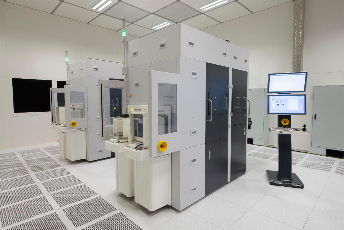
Picture: The EVG7300 SmartNIL nanoimprint and wafer-level optics system, which combines multiple UV-based process capabilities in a single platform.
“With more than 20 years of experience in nanoimprint technology, EV Group continues to pioneer this critical field to develop innovative solutions to meet our customers’ evolving needs,” says corporate technology director Thomas Glinsner. “The latest introduction to our family of nanoimprint solutions, the EVG7300, combines our SmartNIL full-field imprint technology with lens molding and lens stacking in a state-of-the-art system with the most precise alignment and process parameter control on the market — providing our customers with unprecedented flexibility for their industry research and production needs.”
The EVG7300 system is offered as both a stand-alone tool as well as an integrated module in EVG’s HERCULES NIL fully integrated UV-NIL track solution, where additional pre-processing steps (such as cleaning, resist coating and baking or post-processing) can be added to optimize for particular process needs. The system features alignment accuracy down to 300nm, which is enabled by a combination of alignment stage improvements, high-accuracy optics, multi-point gap control, non-contact gap measurement and multi-point force control.
The EVG7300 is a highly flexible platform that offers three different process modes (lens molding, lens stacking and SmartNIL nanoimprint) and support for substrate sizes ranging from 150mm to 300mm wafers. Quick loading of stamps and wafers, fast alignment optics, high-power curing and a small tool footprint enable what is said to be a highly efficient platform capable of serving the industry’s manufacturing needs for emerging WLO products.
EVG is accepting orders for the system, and product demonstrations are now available at the firm’s NILPhotonics Competence Center at its headquarters.
EVG at SPIE AR/VR/MR 2022
EVG is giving an invited talk on the benefits of NIL in manufacturing augmented reality waveguides at the SPIE AR/VR/MR Conference and Exhibition, co-located with SPIE Photonics West, at the Moscone Center in San Francisco (22-27 January). EVG is also exhibiting at the event, showcasing its manufacturing solutions for optical and photonic devices and applications.


