


News: Microelectronics
3 February 2022
NiO/Ga2O3 heterojunction power
Hebei Semiconductor Research Institute and Nanjing University in China claim the highest Baliga figure of merit (FOM) achieved so far among all reported β-gallium oxide (Ga2O3) diodes [Yuangang Wang et al, IEEE Transactions on Power Electronics, v37, p3743, 2022].
The 5.18GW/cm2 FOM comes in at about 15% of the theoretical limit for Ga2O3 of 34GW/cm2, based on material properties. The device also surpassed reported silicon carbide (SiC) limits for diodes for the first time. The theoretical limit for SiC is 3.35GW/cm2, calculated by the team, based on the references ([1] B. J. Baliga, Wide Bandgap Semiconductor Power Devices, Woodhead Publishing, 2019, p4; [2] Masataka Higashiwaki et al, Gallium Oxide Materials Properties, Crystal Growth, and Devices, Springer, 2020, p8).
The ultra-wide bandgap of Ga2O3 leads to expectations of a very high critical field for breakdown. Ga2O3 also has prospects arising from lower potential production costs, along with commercial availability of Ga2O3 in substrate form.
The devices (Figure 1) used a pn heterojunction structure of a thin p-type nickel oxide (p-NiO) layer on n-type Ga2O3. In addition, a junction termination extension (JTE) and a small-angle beveled field-plate (BFP) were used to control electric field crowding effects. Such structures reduce the peak field and allow higher breakdown voltages to be reached.
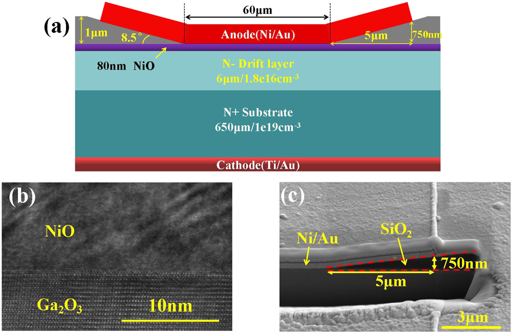
Figure 1: Schematic cross-section of (a) NiO/Ga2O3 HJD with JTE and small-angle BFP, (b) cross-sectional high-resolution transmission electron microscope images of NiO/Ga2O3 interface, and (c) cross-sectional scanning electron microscope images of BFP structure.
The Baliga FOM represents the leading trade-off between breakdown voltage and specific on resistance in the combination Vbr2/Ron,sp.
The drift layer of the device was grown on heavily n-type Ga2O3 substrate using halide vapor phase epitaxy (HVPE). The electron concentration from tin doping of the substrate was 1x10¹⁹/cm3. The 6μm drift layer had a much lower electron concentration of 1.8x10¹⁶/cm3.
The 80nm polycrystalline NiO layer was applied by 150W radio frequency (RF) magnetron sputtering in argon/oxygen atmosphere at room temperature. Hall measurements showed the layer to be p-type with a hole concentration of 2.5x10¹⁸/cm3 with 0.53cm2/V-s mobility. The NiO layer was covered with silicon dioxide (SiO2) from plasma-enhanced chemical vapor deposition (PECVD).
The beveled field-plate was formed from variable-temperature (90-145°C) photoresist reflow and inductively coupled plasma etch of the SiO2 layer. The bevel angle was about 8.5°.
The back ohmic contact came from electron-beam evaporation and rapid thermal annealing (RTA) in nitrogen of titanium/gold (Ti/Au). The Ni/Au anode was formed in a lift-off process. The field-plate was around 5μm thick. The anode area was 60μmx60μm.
The researchers also produced Ga2O3 Shottky barrier diodes (SBDs) and heterojunction diodes (HJDs) without JTE and/or beveled field-plate.
The SBD had the lowest Ron,sp of 1.09mΩ-cm2, while it was 1.23mΩ-cm2 for an HJD without junction termination extension or beveled field-plate. The JTE and BFP reduced Ron,sp for HJDs to 1.12mΩ-cm2. The turn-on voltage of the HJDs was around 1.6V (giving 1A/cm2 current density), higher than for the SBD. Also, the ideality of the HJDs was higher at 1.38/1.20 without/with JTE and BFP, compared with 1.08 for the SBD.
Although the SBD seems preferable so far, the HJD, with its higher barrier and deeper depletion junction depth, is likely to be more resilient under ultra-high voltage stress. Without JTE/BFP the reverse-bias breakdown for the HJD came in at 955V, relative to 460V for SBDs. Adding a JTE increases this to 1945V. The full JTE/BFP package gave a further boost to 2410V.
The researchers are still working on challenges for the delivery of large-size devices with controllable performance and robust reliability. These challenges concern the uniformity of the Ga2O3 epitaxial wafer and sputtered NiO layer, especially in terms of thickness, concentration, and defect density.
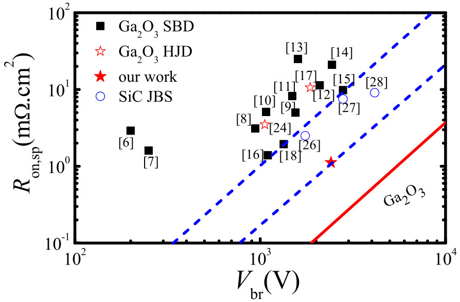
Figure 2: Plot of Ron,sp versus Vbr for reported vertical β-Ga2O3 and SiC diodes. Red solid star represents Hebei/Nanjing record. Diagonal lines represent equal Baliga FOMs, including Ga2O3 theoretical limit.
Despite the challenges, the Baliga figure of merit of the JTE/BFP HJD reached a record 5.18GW/cm2 (Figure 2).
β-gallium oxide diodes GaO HVPE PECVD
https://doi.org/10.1109/TPEL.2021.3123940
The author Mike Cooke is a freelance technology journalist who has worked in the semiconductor and advanced technology sectors since 1997.


