


News: Microelectronics
8 October 2021
University of New Mexico creates first monolayer silicon carbide
Professor Sakineh Chabi of the University of New Mexico and her team have discovered what is reckoned to be the first monolayer silicon carbide (Sakineh Chabi et al, ‘The Creation of True Two-Dimensional Silicon Carbide’, Nanomaterials (2021) 11(7), 1799). The newly discovered 2D SiC materials have a graphene-like hexagonal lattice, and average thickness of 0.25nm (see Figure).
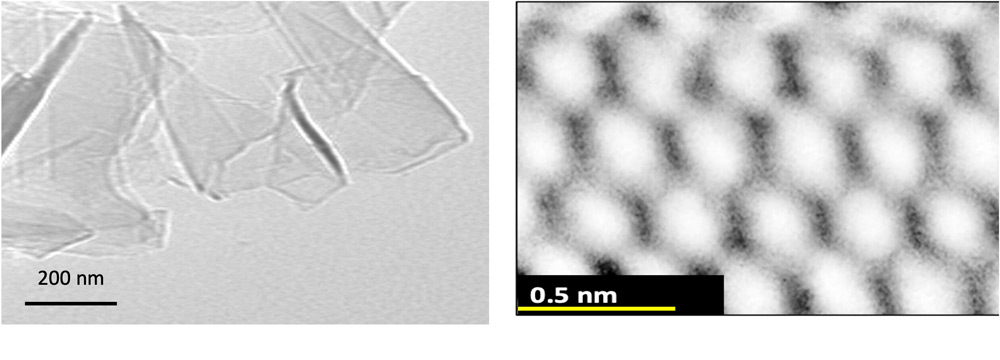
Picture: Transmission electron microscopy images of the exfoliated two-dimensional silicon carbide nanosheets. (Courtesy of Sakineh Chabi.)
Theoretical studies have predicted that 2D SiC has a stable graphene-like honeycomb structure and is a direct-bandgap semiconducting material. Experimentally, however, the growth of 2D SiC has challenged scientists for decades because bulk silicon carbide is a strong covalently bonded material. Adjacent atoms of SiC bond together via covalent sp3 hybridization, which is much stronger than van der Waals bonding in layered materials. Additionally, bulk SiC exists in more than 250 polytypes, further complicating the synthesis process, and making the selection of the SiC precursor polytype extremely important.
Chabi led her team to demonstrate, for the first time, the successful isolation of 2D SiC from bulk SiC via a top-down approach (specifically, a wet exfoliation method). Unlike many other 2D materials such as silicene that suffer from environmental instability, the created 2D SiC nanosheets are environmentally stable, and show no sign of degradation.
2D SiC also shows interesting Raman behavior, different from that of the bulk SiC. Results suggest a strong correlation between the thickness of the nanosheets and the intensity of the longitudinal optical (LO) Raman mode. Furthermore, the created 2D SiC shows visible-light emission, indicating its potential applications for light-emitting devices and integrated microelectronics circuits.
As a wide-bandgap semiconducting material with high thermal capability and high voltage breakdown, SiC is a leading material for high-power electronics, high-temperature applications, and quantum information processing. For example, SiC is considered to be the ideal material solution for the post-Moore era. However, the created 2D SiC material should outperform bulk SiC in several ways. As a result of reduced dimensionality, 2D SiC possesses an unusual set of electronic, optical and structural properties, such as a direct wide-bandgap feature and angstrom-level thickness, which are very important for next-generation semiconductors. Given the high maturity of SiC technologies (e.g. SiC wafers), the potential to convert 2D SiC to a real device is enormous, reckon the researchers.


