


News: LEDs
15 October 2021
Relaxed InGaN for green/red light emission
University of California Santa Barbara (UCSB) in the USA has reported a simpler process for producing relaxed indium gallium nitride (InGaN) pseudo-substrates with a view to more efficient long-wavelength light-emitting devices in the green (500-565nm) and red (625-700nm) wavelength ranges [Philip Chan et al, Appl. Phys. Lett., v119, p131106, 2021]. Up to now, attempts to reduce strain in InGaN layers have been quite complex. The UCSB method used just MOCVD.
The work aimed to reduce the strain in InGaN layers and allow higher-temperature growth. Indium incorporation in GaN is reduced in strained material, an effect referred to as ‘composition pulling’. Lower-temperature growth is normally used to compensate for reduced indium incorporation. For example, red InGaN light-emitting diodes (LEDs) are typically grown by metal-organic chemical vapor deposition (MOCVD) at temperatures ranging from 700 to 765°C.
Unfortunately, low-temperature growth also generates higher defect densities, increases impurity incorporation, and degrades surface morphology. These effects are associated with decreased adatom mobility during MOCVD, along with reduce efficiency in LEDs and lasers.
The researchers see their work as potentially benefiting efforts towards displays based on micro-LEDs (μLEDs), which need red, green and blue emitters. Blue GaN-based LEDs are well established, but increasing indium incorporation for longer wavelengths has been problematic. However, InGaN-based LEDs are attractive for these applications due to less impact from surface recombination effects that particularly hit smaller devices, relative to the standard red-emitting material, aluminium indium gallium phosphide.
The UCSB epitaxial material was grown on (0001) sapphire through MOCVD. The relaxed InGaN pseudo-substrate was achieved by growing a 5.5μm GaN template layer, followed by a 2.5nm 750°C InGaN ‘decomposition layer’ (DL) and a 100nm GaN decomposition stop-layer (DSL).
The growth temperature of the first 30nm of the DSL was 750°C; then the temperature was ramped to 1000°C during the remaining 70nm. The high temperature was designed to both result in a high-quality crystal structure for subsequent growth, and to decompose the underlying InGaN DL, forming voids that would allow an overlying 200nm 920°C In0.04Ga0.96N buffer/pseudo-substrate to relax.
A high-resolution x-ray diffraction (HRXRD) reciprocal-space map (RSM) suggested that the pseudo-substrate consisted of 85%-relaxed In0.04Ga0.96N. “The sample shows deep pitting and poor surface morphology from unoptimized growth temperature and InGaN buffer growth conditions,” the team comments.
The pseudo-substrate was loaded, together with a simple GaN/sapphire template, into an MOCVD reactor to grow further InGaN layers, creating a 4-period multiple quantum well (MQW) structure of 2.5nm/2.5nm 865°C InGaN well/2.5nm GaN cap, along with 8.3nm 900°C InGaN barrier. The researchers comment that the sample on the pseudo-substrate had “a slightly yellow appearance from the increased indium incorporation”. They add: “The decomposed InGaN layer appears dark in the center, possibly from the metallic indium that remains after thermal decomposition during the high-temperature GaN DSL growth.”
Photoluminescence (PL) from 325nm helium-cadmium laser excitation showed peaks at 440nm and 515nm for the MQWs grown on the GaN template and InGaN pseudo-substrate, respectively. Further, the intensity of the peak from the MQW structure on the pseudo-substrate was up to three times stronger than that on GaN. There was variation of intensity and wavelength according to where the MQW was excited for photoluminesence (Figure 1).
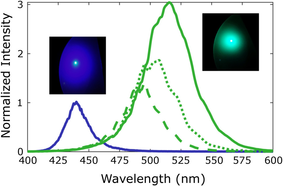
Figure 1: Room-temperature PL emission from MQW regrown on GaN template and relaxed InGaN buffer by thermal decomposition of an InGaN underlayer. Solid lines depict emissions from half-radius of substrate, dotted depicts center, and dashed depicts edge.
The researchers comment: “The wavelength shift could be attributed to the lessening of the compositional pulling effect in the sample with the relaxed buffer.” In other words, the reduced strain allowed more indium to be incorporated into the MQWs, reducing the bandgap energy, increasing the wavelength of the emitted photons. The increased light intensity was attributed to better light extraction due to the rough surface reducing total internal reflection back into the epitaxial material.
Material for a red LED was grown in a similar way except the DL, DSL and buffer layers were doped n-type with silicon. Also, the MQW was grown at 825°C with 6nm GaN barriers rather than the thicker GaN/InGaN combination. The 920°C p-contact layers consisted of 80nm p-In0.04Ga0.96N and 12nm more heavily doped In0.04Ga0.96N. The MOCVD was carried out without interruption between the pseudo-substrate and MQW layers. The p-type layers were activated with 650°C annealing. The metal contacts consisted of indium dots used for electrical probing.
The electroluminescence from this device peaked at 622nm wavelength when the current injection was 20A/cm2 (Figure 2). The full-width at half-maximum (FWHM) was 77nm. The researchers describe the performance of the LED as “quite poor”, due to surface morphology of the buffer layer being rough and pitted. Also, the LED structure was basic, without optimizations such as electron-blocking layers or defect-reduction strategies (e.g. underlying superlattices).
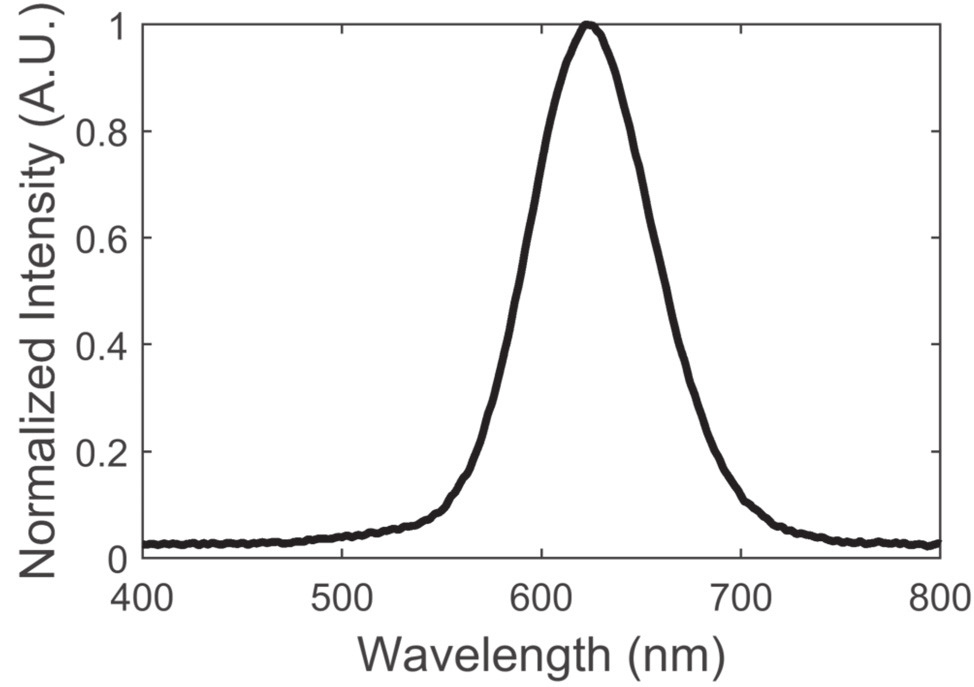
Figure 2: Room-temperature electroluminescence spectrum of red LED at 20A/cm2 current density.
The researchers managed to reduce the surface roughness of a 90%-relaxed In0.025Ga0.975N-buffer pseudo-substrate recipe to 1.3nm root-mean square. This was grown with the low-temperature portion of the GaN DSL reduced to 4nm. The high-temperature portion was thickened to 150nm, grown at 1150°C in hydrogen. Also, the buffer was more complex: 50 periods of 16nm 950°C InGaN with 2nm/2nm GaN interlayers grown at 950/1000°C. The lower-temperature growth used nitrogen ambient. The high-temperature step included 5% hydrogen carrier, which was designed to fill any v-pits that were formed. The team hopes to extend this better morphology to higher indium contents.
InGaN LEDs Lasers MOCVD Pseudo-substrate
https://doi.org/10.1063/5.0064755
The author Mike Cooke is a freelance technology journalist who has worked in the semiconductor and advanced technology sectors since 1997.


