


News: Optoelectronics
5 October 2021
HKUST demonstrates high-performance photodetector grown on SOI for silicon photonics
A team led by professor Kei-May Lau of the Department of Electronic and Computer Engineering at Hong Kong University of Science and Technology (HKUST) has developed a novel semiconductor deposition scheme and demonstrated high-performance photodetectors (PDs) grown on silicon-on-insulators (SOI) for silicon photonics (Ying Xue et al, ‘High-performance III-V photodetectors on a monolithic InP/SOI platform’, Optica, 14 September 2021). The III-V photodetectors are qualified candidates for high-speed data communications in silicon photonics. The results point to a practical solution for the monolithic integration of III-V active devices and silicon-based passive devices on the SOI platform in the future.
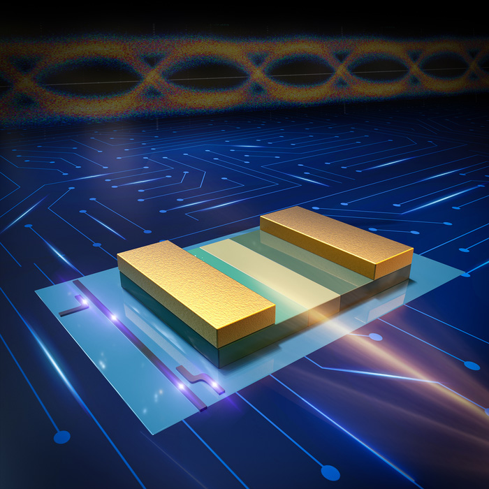
Picture: Fabricated high-performance III-V photodetector on a monolithic InP/SOI platform for application in silicon photonics (courtesy of Hong Kong University of Science and Technology).
With ever-growing communication traffic pushing the conventional electronic interconnection to the limit, silicon photonics is regarded as an enabling solution due to its high-speed and large bandwidth capability, as well as scalable and high-throughput manufacturing. High-performance photodetectors are crucial optical building blocks in silicon photonic integrated circuits (Si-PICs). In addition to characteristics such as high responsivity, low dark current, large bandwidth, operation over a wide wavelength band, efficient light coupling with silicon waveguides and CMOS compatibility are also needed for the photodetectors.
III-V photodetectors have long been deployed in indium phosphide (InP)-based photonic integrated circuits (PICs) because of their superior device performance. Recently, interest in III-V photodetectors grown on silicon began to flourish, complementing the research on integrating III-V lasers on silicon and the eventual goal of having high-performance III-V photonics integrated on the silicon photonics platform. For the III-V photodetectors on silicon realized using the traditional blanket hetero-epitaxy method, the thick buffer layers used for defect reduction make it challenging for light coupling with silicon waveguides, and the reported 3dB bandwidths of these photodetectors often fall in the range of sub-10GHz.
HKUST developed the lateral aspect ratio trapping (ART) method to grow III-V materials on SOI without the need for thick buffers. III-V photodetectors grown on SOI using this method feature an in-plane configuration with the silicon device layer, which allows easy integration of the photodetectors and silicon waveguides. The team designed and fabricated III-V photodetectors with a variety of dimensions on a monolithic InP/SOI platform, also developed by the team.
The photodetectors feature a large 3dB bandwidth exceeding 40GHz, a high responsivity of 0.3A/W at 1550nm and 0.8A/W at 1310nm, a wide operation wavelength span over 400nm, and a low dark current of 0.55nA. The photocurrent is adjustable for various applications by varying the length of the photodetectors. Design of interfacing these photodetectors with silicon waveguides can be flexible and simple.
For the first time, the team has demonstrated III-V photodetectors grown on the monolithic InP/SOI platform (paper to appear in Light: Science and Application) to fulfill the stringent criteria for photodetectors in silicon photonics. “This was made possible by our latest development of a monolithic InP/SOI platform with both sub-micron InP bars and large-dimension InP membranes,” says Lau. “Our team’s combined expertise and insights into both device physics and growth mechanisms allow us to accomplish the challenging task of cross-correlated analysis of epitaxial growth, material characteristics and device performance.”
The work is a collaboration with a research team led by professor Hon-Ki Tsang of the Department of Electronic Engineering at Chinese University of Hong Kong (CUHK).
The device fabrication technology was developed at HKUST’s Nanosystem Fabrication Facility (NFF) on Clear Water Bay campus. The work is supported by Research Grants Council of Hong Kong and Innovation Technology Fund of Hong Kong.
First bufferless 1.5μm III-V lasers grown directly on silicon wafers in Si-photonics
Optical Society names Kei May Lau as recipient of 2020 Nick Holonyak Jr Award


