


News: Optoelectronics
18 November 2021
InP-lithium niobate hybrid laser
Sun Yat-sen University in China and University of British Columbia in Canada claim the first electrically pumped hybrid lithium niobate/III-V laser [Ya Han et al, Optics Letters, v46, p5413, 2021]. The device consisted of an indium phosphide (InP) optical gain chip butt-coupled to a lithium niobate (LiNbO3) on insulator (LNOI) photonic integrated circuit (PIC). The hybrid laser achieved a 36nm tuning range in the O-band infrared optical communication range (1260-1360nm).
Lithium niobate (LN) features a wide transparent bandwidth, and high electro-optic and second-order nonlinear optical coefficients. The researchers believe that integrating an LNOI modulator section to the hybrid laser could pave the way to a fully integrated optical transmitter beyond 100gigabit/second data rates for wavelength-division multiplex (WDM) systems. WDM requires electrically pumped tunable single-mode lasers.
The light of the hybrid laser was generated in an InP-based reflective semiconductor optical amplifier (RSOA), coated to provide an anti-reflective front facet (<0.01% reflection), and partially reflective (~10%) rear facet. The front facet was tilted 8° to further reduce back reflection into the RSOA, avoiding lasing just within the InP device.
The LNOI PIC (Figure 1) included a spot size converter (SSC) to couple the light from the RSOA efficiently. The complete 5.18mm-long Fabry-Pérot laser cavity was between the rear partially reflective facet of the RSOA and a distributed Bragg reflector (DBR) on the LNOI PIC.
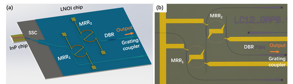
Figure 1: (a) Schematic for tunable hybrid LN/III-V laser using LNOI PIC for laser feedback; (b) microscope image of fabricated LNOI PIC.
The laser wavelength was tuned by two cascaded micro-ring resonators (MRRs) with slightly different free spectral range, using a Vernier filter effect. The laser wavelength was altered by heating the MRRs.
The researchers used LNOI with x-cut LN crystal orientation. The LNOI wafer consisted of 360nm LN layer, 4.7μm thermal silicon dioxide insulator, and 500μm silicon substrate. Patterning of the LN consisted of electron-beam lithography and inductively coupled plasma etch. This patterning was carried out in two steps: the first creating the waveguide, and the second the inverse tapered structure for off-chip coupling.
The LNOI fabrication was completed with plasma-enhanced chemical vapor deposition (PECVD) of 1μm silicon dioxide, lift-off processing of nickel-chromium with gold contact pads for the heaters, and polishing the facet for efficient light coupling to the RSOA.
The beam from the RSOA chip was elliptical with 1.98μmx0.99μm waist. The SSC was a bilayer inverse taper design with the bottom layer being a trident waveguide, and the top was a butt-coupling interface. The light was output through a grating coupler.
The threshold current for lasing at 1331.88nm wavelength was 100mA, corresponding to 2.5kA/cm2 density. The maximum output power was 2.5mW, at 300mA injection. The output power was limited by the leakage from the back facet of the RSOA, while the DBR had 90% reflection to ensure lasing. Unfortunately, the researchers’ setup did not allow light collection from the RSOA’s back facet.
The light output power did not increase monotonically, since there was mode hopping as the current increased. At 200mA, the light output was at 1325.5nm wavelength with single-mode suppression ratio (SMSR) higher than 60dB.
By variously heating the MRRs, a wide range of wavelengths, 1.3045–1.3409μm, was achieved (Figure 2). For all these wavelengths, the SMSR was more than 43dB with 200mA injection.
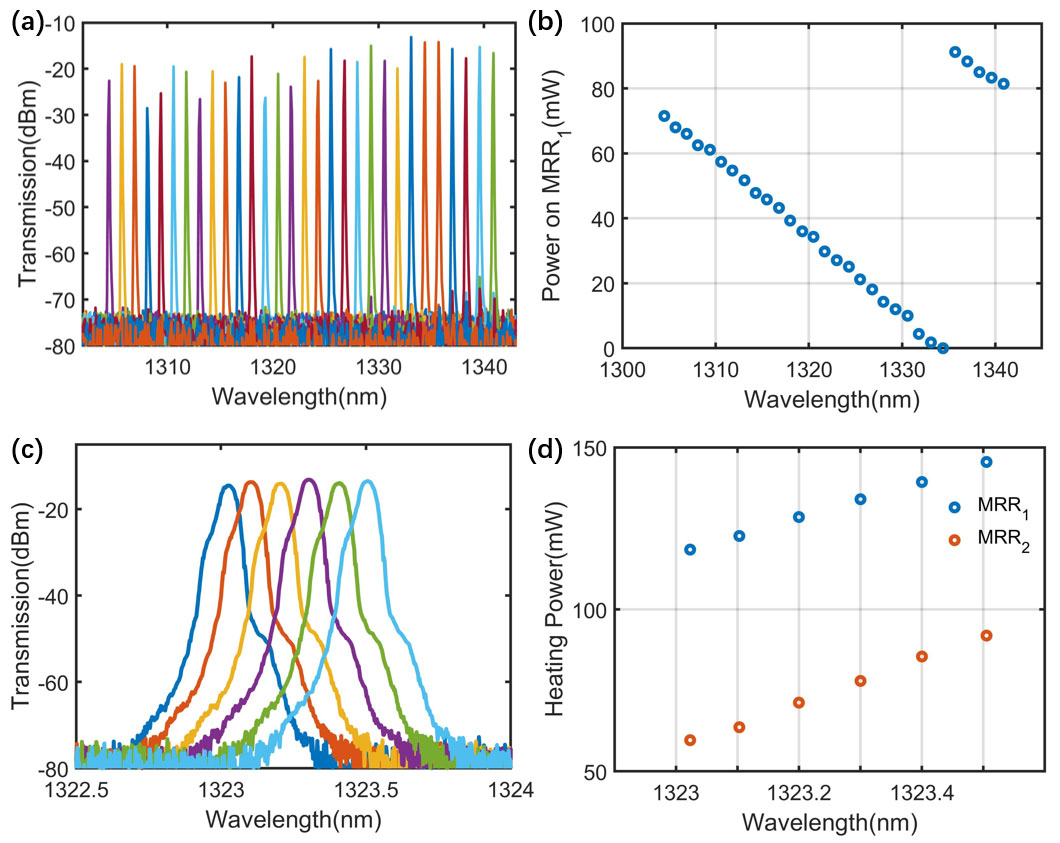
Figure 2: Superimposed spectra of (a) coarse tuning and (b) corresponding lasing wavelength and heating power on MRR1. Superimposed spectra of (c) fine tuning and (d) corresponding lasing wavelength and heating power on MRR1/MRR2.
The team comments that the results achieved were comparable with the performance of state-of-the-art combinations of InP RSOAs with other PIC technologies using silicon (1.647–1.69μm wavelength range) or silicon nitride (1.524–1.568μm) waveguide materials. The InP-LNOI combination also had a wider wavelength range and higher SMSR than a monolithic III-V O-band laser (1.2802–1.312μm, 52dB peak SMSR). The monolithic laser did have much higher output power: 7.8mW, compared with 2.5mW for the LNOI hybrid.
The researchers point out that the low rear facet reflectivity suggests that much better performance can be reached by increasing from a measly 10% to 90%. “Furthermore, reducing the coupling loss between the RSOA and LNOI chip can further improve the on-chip output power,” they add.
InP-lithium niobate hybrid laser InP LiNbO3 PIC PECVD
https://doi.org/10.1364/OL.442281
The author Mike Cooke is a freelance technology journalist who has worked in the semiconductor and advanced technology sectors since 1997.


