


News: Microelectronics
27 May 2021
GaN breakdown reaches beyond 10kV
Researchers based in the USA and China claim the highest breakdown voltage so far, more than 10kV, for gallium nitride (GaN) power devices [Ming Xiao et al, IEEE Electron Device Letters, vol42, p808, 2021].
The team from Virginia Polytechnic Institute and State University in the USA and Enkris Semiconductor Inc in China fabricated multi-channel Schottky barrier diodes (SBDs) with a p-GaN reduced surface field (RESURF) structure, targeted at reducing the peak electric field and hence extending the breakdown capability. At the same time, the multi-channel structure reduces on-resistance.
The researchers see their work as potentially contributing to the future needs of renewable-energy generation, industrial motor drives, the electricity grid, and transportation. Competing silicon and silicon carbide (SiC) technologies suffer from slow switching speeds or exorbitant costs, respectively.
The device material consisted of 20nm p+-GaN and 350nm p-GaN top layers over a 5x multi-channel of 23nm Al0.25Ga0.75N/100nm intrinsic GaN. The material was grown continuously, avoiding regrowth in fabrication, on sapphire, using metal-organic chemical vapor deposition (MOCVD).
Hall measurements on the material demonstrated a sheet resistance of 178/Ω/square, 2010cm2/V-s mobility, and a 1.75x10¹³/cm2 five-channel total two-dimensional electron gas (2DEG) density. The 2DEG density included the depletion effect of having an overlying p-GaN layer.
The device fabrication process (Figure 1) began by forming a self-aligned ohmic cathode contact with titanium/aluminium/nickel/gold. The isolation mesa height was 900nm. The anode contact was nickel/gold with a 2μm extension (LA). The contacts were wrapped around the mesa sidewalls to give a good contact with the multi-channel.
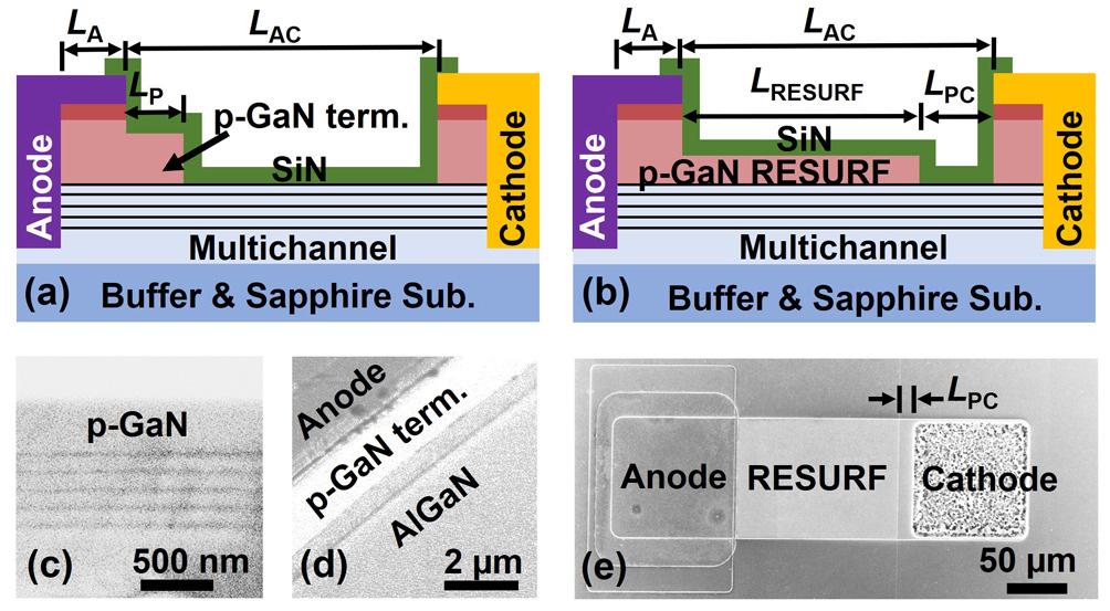
Figure 1: Schematics of multi-channel AlGaN/GaN SBD with (a) p-GaN edge termination and (b) p-GaN RESURF. Cross-sectional scanning electron microscope images of (b) p-GaN/multi-channel region, (c) p-GaN edge termination region, (d) top-view of p-GaN RESURF (LAC = 123μm) before SiNx passivation.
The p-GaN material was mainly etched away, leaving either a 2μm termination structure (LP) or the RESURF structure. The thickness of the p-GaN in the RESURF region was aimed at balancing the positive charges in the p-GaN against the negative carriers in the 2DEG multi-channel. The critical thickness required for this was determined using capacitance-voltage measurements on test structures. The optimal value was found to be in the range 80-100nm.
The team sees their RESURF structure as being more practical in terms of fabrication, compared with ‘polarization superjunction’ (PSJ) devices, which use charge polarization effects to balance the charge. Ideal PSJs would not need a RESURF structure. However, the world is not ideal, and net charge tends to appear in multi-channel devices due to unintentional donor doping.
The researchers comment: “Actually, the RESURF multi-channel structure proposed in this work shows an effective design for an unbalanced PSJ device, while the ideal multi-channel PSJ device may be very difficult to realize experimentally.”
The fully etched region of the RESURF diode up to the cathode was 12μm (LPC). The final silicon nitride (SiNx) passivation was applied using plasma-enhanced chemical vapor deposition (PECVD). The 1mA/mm current density turn-on voltage for the devices was 0.6V. The 3V on/off current ratio was ~107.
The RESURF structure was found to give ~2x higher breakdown compared with diodes without termination and ~1.5x higher than for those with p-GaN termination. The researchers rinsed the devices in Fluorinert FC-70 during the breakdown experiments.
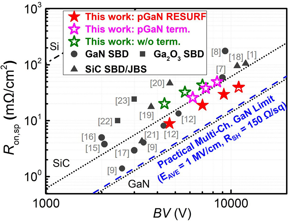
Figure 2: Differential RON,SP versus BV benchmarks for the presented SBDs and state-of-the-art GaN, SiC, and gallium oxide (Ga2O3) high-voltage SBDs. Dotted lines show indicated theoretical limits.
In terms of the average breakdown lateral electric field, the RESURF devices demonstrated values in the range 0.94-1MV/cm, compared with 0.42-0.47MV/cm for devices without termination, and 0.59-0.64MV/cm with. The breakdown was catastrophic rather than avalanche.
A RESURF device with anode-cathode distance (LAC) of 98μm demonstrated a breakdown voltage of 9.15kV, and a 123μm device showed no degradation up to the 10kV limit of the researchers’ equipment. The leakage of the latter device at 10kV reverse bias was 1.8x10⁻⁵A/mm. The team suggests that the average breakdown electric field values of the shorter-drift-region devices would suggest a breakdown voltage of ~11kV.
Since the RESURF structure is larger than the termination structure, one expects a higher parasitic capacitance. Integrating capacitance-voltage measurements up to 3kV reverse bias gave a total capacitive charge of the RESURF structure of 2.1nC/mm, compared with 1.7nC/mm for the terminated devices. However, the switching loss from the extra capacitance was found to increase by just 5%, since most of the capacitive charge is removed at low reverse bias. The capacitive energy loss in the RESURF device was calculated to be 1.6μJ/mm.
Simulations suggest that the effect of the RESURF structure was to spread the electric field more uniformly over the lateral drift region rather than peaking/crowding near the anode. In the simulations, the peak electric field was more than 5MV/cm for the 123μm terminated devices at 10kV reverse bias, and 3.5MV/cm for the comparable RESURF structure.
The Baliga figure of merit (BV2/RON,SP), which balances breakdown voltage against the specific on-resistance penalty of longer drift regions, was more than 2.8GW/cm2 for the 4.6-10kV RESURF devices. The 98μm device demonstrated a 2.84GW/cm2 figure of merit.
The researchers comment that this is “the highest among all reported 5kV+ SBDs” and “well exceeds” the 1-dimensional silicon carbide (SiC) unipolar theoretical limit. The team also points out that 4-inch GaN-on-sapphire wafers are around 2-3x lower cost, compared with 4-inch SiC. They add: “Together with a much smaller die size, the material cost of our GaN SBDs is expected to be much lower than similarly rated SiC SBDs. The processing cost of lateral GaN devices is also expected to be lower than SiC.”
The team estimated the switching figure of merit - the product of the 80mA/mm forward voltage and the total capacitive charge - at 15.7nCV for a 10kV 0.3A RESURF device, compared with 30.8nCV for a commercial 3.3kV 0.3A SIC SBD.
Schottky barrier diode MOCVDi GaN SiC
https://doi.org/10.1109/LED.2021.3076802
The author Mike Cooke is a freelance technology journalist who has worked in the semiconductor and advanced technology sectors since 1997.


