


News: Microelectronics
25 March 2021
Ultraviolet shines for AlN conductivity
Researchers at North Carolina State University (NCSU) and Adroit Materials in the USA have boosted free-electron concentration and hence conductivity in silicon-implanted aluminium nitride (AlN) by using ultraviolet (UV) illumination during the activation anneal [M. Hayden Breckenridge et al, Appl. Phys. Lett., vol118, p112104, 2021].
AlN has an ultra-wide bandgap of 6.1eV, which is an attractive property for high-power and high-voltage electronics, along with the potential for deep-UV optoelectronics in the ~200nm wavelength range. Wide-bandgap materials are challenging in terms of enabling high electrical conductivity.
Improving conductivity in AlN involves reducing the densities of threading dislocations and aluminium vacancy-silicon (VAl-nSi) complexes. These defects reduce the effectiveness of silicon as a doping agent through trapping electrons, ‘self-compensation’, of the shallow ~70meV donor state, reducing conductivity.
The UV illumination was designed to generate excess minority carriers whose presence shifted the formation energy of VAl-nSi complexes upwards, reducing their density. The generation of holes needed UV photons with energies higher than the 6.1eV bandgap (i.e. wavelengths shorter than 200nm). The theoretical designation of the technique is ‘defect Quasi Fermi Level’ (dQFL) control.
The researchers used AlN substrates with a low dislocation density of less than 103/cm2. The single-crystal AlN was processed from boules grown by physical vapor transport (PVT). A homoepitaxial AlN layer was added by using nitrogen-rich metal-organic chemical vapor deposition (MOCVD).
The n-type doping was through silicon ion implantation with 1014 atoms/cm2 at 100keV energy. The AlN substrate was tilted at 7° during implantation to avoid the channeling effects of ions easily passing through aligned gaps in the lattice structure.
The doping was activated through annealing at 1200°C for 2 hours in nitrogen at 100Torr pressure. The temperature is viewed as being low, below the value needed for the system to reach thermodynamic equilibrium.
The sample was illuminated with UV light from a 1kW mercury-xenon lamp. The UV illumination decreased mid-gap photoluminescence (Figure 1), suggesting successful suppression of the generation of compensating VAl-nSi point defects during post-implant annealing.
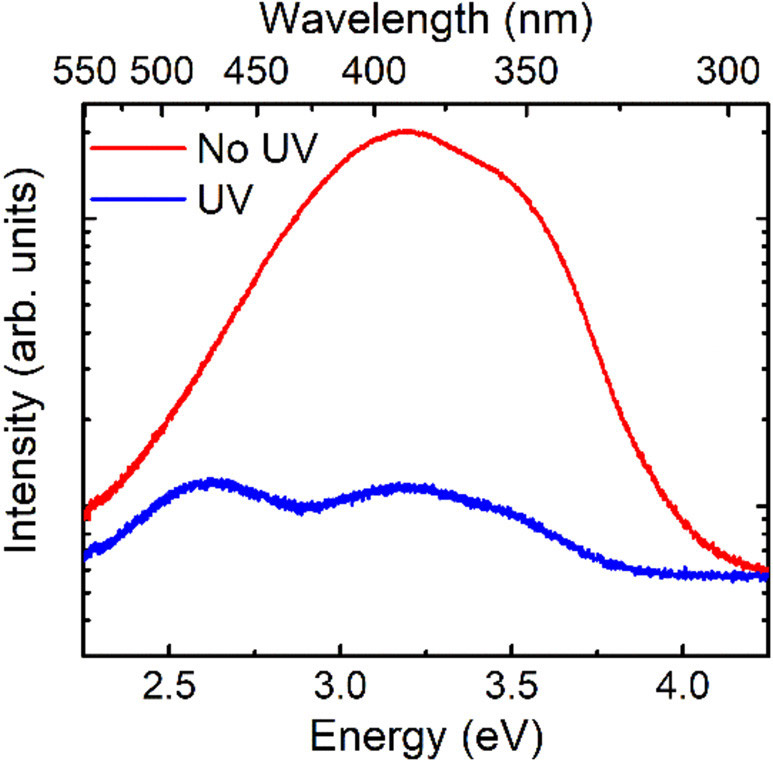
Figure 1: Room-temperature photoluminescence spectra for Si-implanted AlN annealed without (red) and with (blue) UV illumination.
The contacts for electrical measurements were electron-beam evaporated vanadium/aluminium/nickel/gold in a van der Pauw format. The contacts were annealed after deposition at 850°C for a minute in nitrogen.
Conductivity for samples annealed under various samples was measured at a range of temperatures between 300K (room temperature) and 725K (Figure 2). The UV-annealed sample demonstrates a factor of 30 improvement in conductivity across the temperature range, compared with samples annealed at the same temperature but without UV. Higher annealing temperatures closer to ‘equilibrium’ showed worse performance as room temperature was approached.
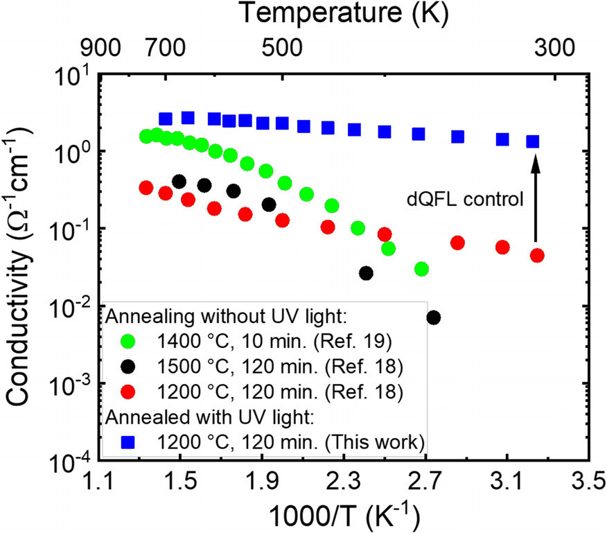
Figure 2: Temperature-dependent conductivities for Si implanted AlN samples annealed with and without UV light at various temperatures.
Using the temperature dependence of the conductivities, the researchers estimated the compensation ratio of the UV-illuminated sample at 0.2, compared with 0.9 for the sample annealed at 1200°C without UV.
Room-temperature Hall measurements were not expected to give reliable results due to the implants giving a Gaussian donor concentration and mobility varying with depth. Hence hot-probe AC measurements were performed.
At temperatures above 400°C, the free-electron concentration was estimated at 5x10¹⁸/cm3 (assumed averaged over a 200nm layer) with a 1cm2/V-s mobility. The sheet carrier concentration was ~1x10¹⁴/cm2 close to the silicon dose.
The researchers comment: “Although a high conductivity exceeding 1/Ω-cm at room temperature was demonstrated in AlN by ion implantation, the measured carrier mobility was about 100 times lower than that can be achieved in the epitaxial doping despite the low compensation ratio.”
The sample 1200°C annealed without UV had a sheet carrier concentration ~1x10¹³/cm2 at a similar mobility. The low mobility is something that one would clearly like further information on in the hope that it could be improved, allowing for even higher conductivity.
https://doi.org/10.1063/5.0042857
The author Mike Cooke is a freelance technology journalist who has worked in the semiconductor and advanced technology sectors since 1997.


