


News: Suppliers
2 March 2021
Eta unveils GaN wafers for laser diode manufacturing
Eta Research of Shanghai, China, which was founded in 2015 to develop free-standing gallium nitride (GaN) wafers, is now producing free-standing GaN wafers at sizes of 2” and 4”, with conductivity available in either silicon (Si)-doped n-type or carbon (C)-doped semi-insulating. The properties of the GaN wafers have been engineered to meet the requirements for laser diode manufacturers.
The wafer orientation flat must be closely aligned to the GaN m-plane, since lasers may be manufactured by cleaving on the crystallographic plane. Eta has therefore developed the process to achieve 0.0±0.1° alignment of the orientation flat to the crystallographic plane.
The typical x-ray diffraction (XRD) rocking curve full width at half maximum (FWHM) for both (002) and (102) are in the range 40-50 arcsec. The dislocation density was measured by both cathodo-luminescence (CL) and etch pit methods, and was found to be in the range 5E5-9E5/cm2.
Eta’s standard offcut is 0.5° toward the m-direction and 0.0° toward the a-direction at the center point of the wafer. The center point offcut can be customized in the range 0.2-0.6°.
The lattice radius specification is >10m, and typical values range from 20m to 60m with the shape as concave. The offcut variation can be calculated from the lattice radius. However, since there is a small concave wafer bow, the actual offcut variation is less than would be calculated from the lattice radius. The offcut was measure by XRD with x-ray reflection alignment to the real wafer surface. The offcut variation over a 4” wafer was measured to be 0.06° for both the m-direction offcut and a-direction offcut. For example, the m-direction offcut was 0.47° on one edge and 0.53° on the other edge over the entire 100mm of the wafer.
The gallium (Ga)-face is polished to an average roughness of 0.15nm measured by a 10µm x 10µm atomic force microscope (AFM) scan. The wafer is cleaned in a special process to remove any contamination from the polishing procedure. Removal of trace-metal impurities from the surface was confirmed by total reflection X-rays fluorescence (TXRF).
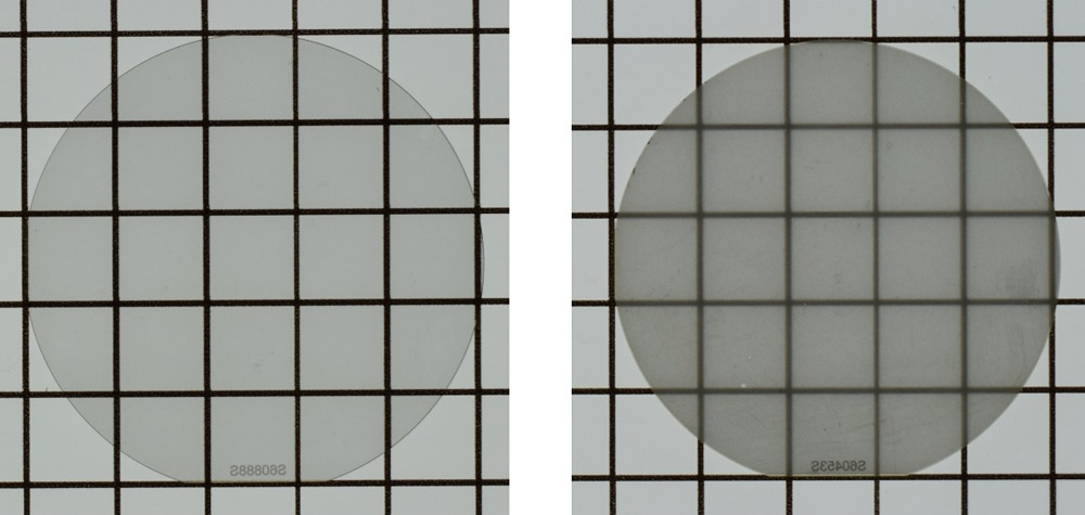
Picture: Left:GaN wafer with backside polished. Right: GaN wafer with backside etched.
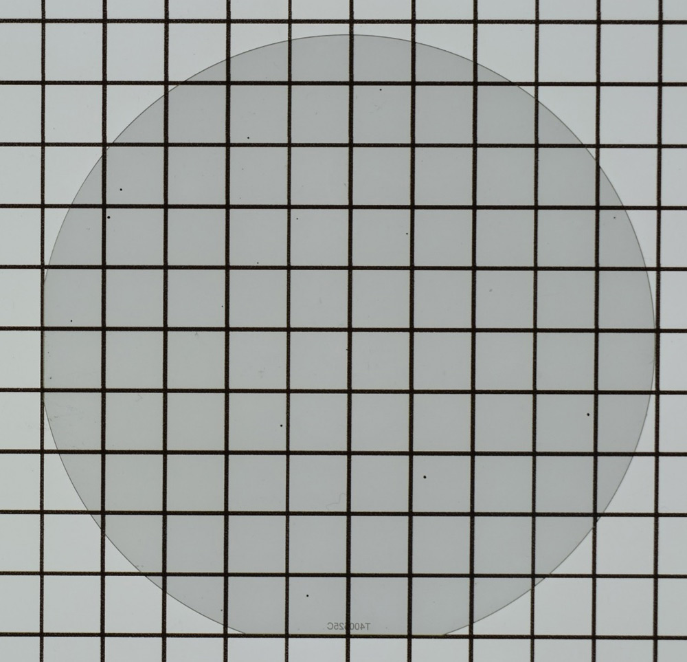
Picture: GaN wafer with backside polished.
The backside finish is available in either polished or etched versions. The average roughness of the backside surface measured by 3D profiler over 239µm x 318µm is 1nm for polished and 1µm for etched. The wafers with polished and etched backside finish are shown in the figures.
Eta demos GaN-on-GaN epitaxy of vertical power device structures
Eta develops 4” semi-insulating GaN wafers
Eta launches polished epi-ready 100mm n-type GaN wafers


