


News: LEDs
4 March 2021
ALLOS’ GaN-on-Si epi used by Toyohashi University for in-vivo neural applications
The team of professor Hiroto Sekiguchi at Japan’s Toyohashi University of Technology together with IP licensing & technology engineering firm ALLOS Semiconductors GmbH of Dresden, Germany have collaborated to realize high-efficiency nitride-based micro-LED chips for novel in-vivo neural applications.
Since their development in the 1990s, nitride LEDs have been saving energy and enabling many new applications, being used ubiquitously in numerous illumination applications and now emerging as micro-LEDs for use in super-large TVs or augmented reality (AR) displays as well as robust automotive displays.
Nitride LEDs for medical applications
Beyond the obvious illumination applications, nitride LEDs are also increasingly proving helpful in medical applications. For example, nitride LEDs emitting ultraviolet light are employed to fight viruses like COVID-19 by disinfecting surfaces.
Another example is Toyohashi University of Technology using nitride micro-LED technology to build medical brain/machine interfaces. Professor Sekiguchi’s group has developed a neural probe to study brain functions using ALLOS’ micro-LED epiwafer. To avoid brain damage, the high efficiency of micro-LEDs is key in order to reduce the harmful impact from heat coming from conversion losses. Furthermore, for micro-LEDs, extreme precision is needed.
GaN-on-Si to overcome manufacturing challenges
For this novel medical application, manufacturing challenges had to been overcome, where ALLOS’ gallium nitride on silicon (GaN-on-Si) technology plays a key role. In particular, it was important to integrate nitride LED technology with mature and precise silicon industry processes in order to achieve highest accuracy and reliability standards.
“We need to achieve extreme precision and reliable results,” says Sekiguchi. “Only industry-grade silicon processing equipment – as we fortunately have at our university – can deliver such processing results. Thus, using ALLOS’ GaN-on-Si epiwafers, which can be processed on silicon lines, was the right choice,” he adds.
“With our CMOS-line-ready GaN-on-Si technologies we unlock the benefits those silicon lines bring – including scalability to 200mm and 300mm for low cost and the exceptionally high reliability and yield levels required for all micro-LED applications,” says ALLOS’ chief technology officer Dr Atsushi Nishikawa.
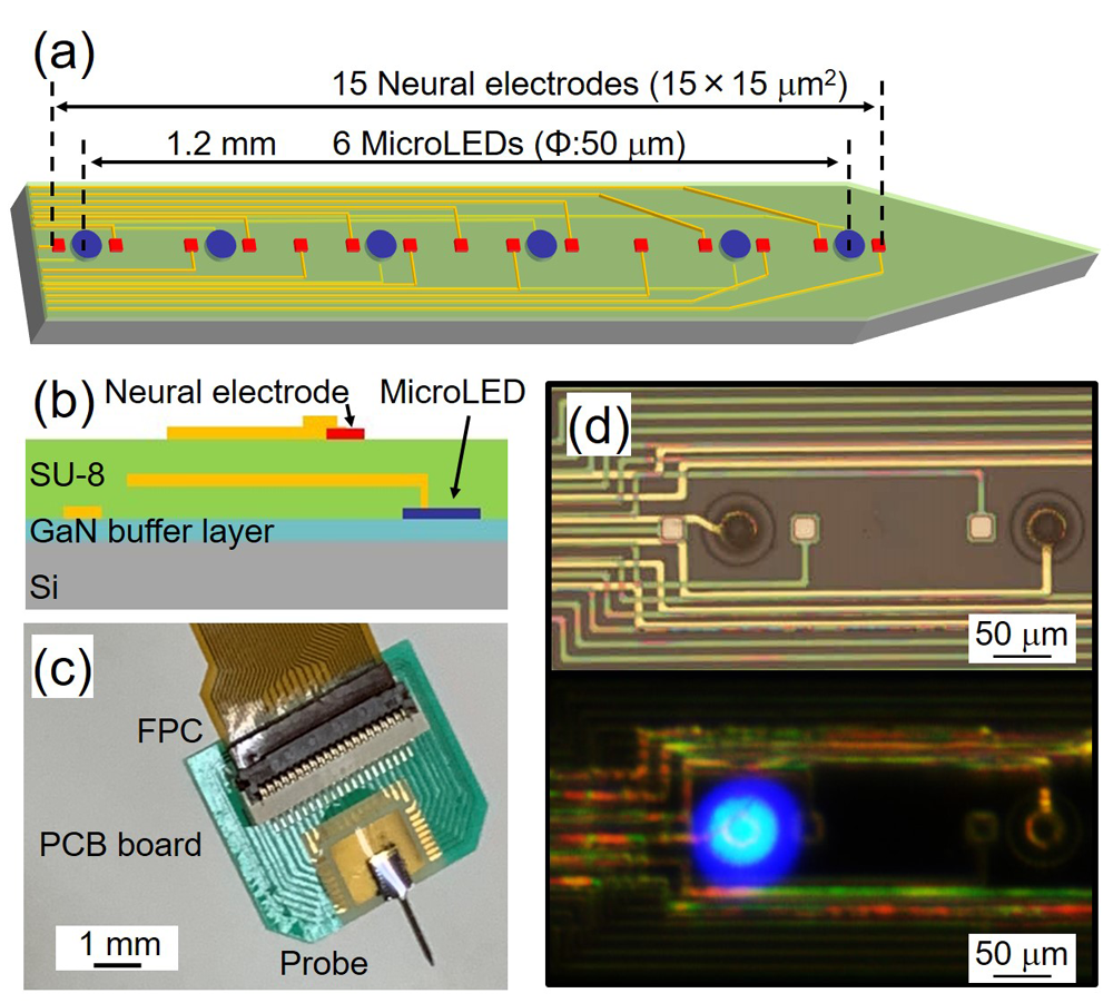
Figure 1: Micro-LED neural electrode probe fabricated by professor Sekiguchi’s group integrating ALLOS’ high-crystal -quality and strain-engineering epiwafer technologies.
At Toyohashi University of Technology, professor Sekiguchi has been working on the development of nitride semiconductor for more than 10 years. Currently, he is considering micro-LEDs as a new optogenetic tool for brain science. Using their silicon process technology and ALLOS’ GaN-on-Si technology, he and his research team are developing a new neural probe that has micro-LEDs for manipulating neural activity and a neural recording electrode for recording neural activity (Hiroki Yasunaga et al, Jpn. J. Appl. Phys. 60, 016503 (2021)). They believe that such a device development will be a powerful tool for opening up new fields of neuroscience.
https://iopscience.iop.org/article/10.35848/1347-4065/abcffa


