


News: Optoelectronics
21 January 2021
CMOS-compatible III-V photodetector
Researchers in Switzerland and the USA have been working to integrate III-V photodetector structures on silicon photonic integrated circuits (PICs) [Yannick Baumgartner et al, Optics Express, vol29, p509, 2021]. The team from IBM Research Zürich, ETH Zürich and IBM T. J. Watson Research Center have developed a process that is compatible with mainstream complementary metal-oxide-semiconductor (CMOS) electronics manufacturing, a key consideration for mass deployment. This means eliminating gold-based contacts and excessive thermal budgets, for example.
The fabricated devices with a 65GHz bandwidth and data reception of 100gigabaud (GBd) benefited from the tunable direct bandgap and high carrier mobility of the indium aluminium gallium arsenide (InAlGaAs) and indium phosphide (InP) III-V materials. These properties should enable “compact high-speed detectors with lower dark currents and transit times, increased photodetection efficiency and thermal stability, decreased footprint and capacitance” without the need for transimpedance amplifiers, according to the researchers.
The team hopes that its work will contribute to achieving the low power consumption of femtojoules/bit targeted for 100gigabits/second optical communications by industry.
The active III-V structure consisted of ten InAlGaAs compressive quantum wells grown on InP by 550°C metal-organic chemical vapor deposition (MOCVD). The structure was wafer-bonded to a Si PIC wafer with an aluminium oxide bonding layer at less than 300°C. The researchers expect the InAlGaAs system to be suitable for devices covering the two main optical communication wavelengths of 1310nm and 1550nm.
The PIC was fabricated in a 220nm silicon-on-insulator (SOI) wafer using hydrogen bromide/oxygen plasma etch in an inductively couple plasma reactive-ion etch (ICP-RIE) tool. The PIC was clad in silicon dioxide and chemical mechanical planarized before the wafer bonding of the III-V material.
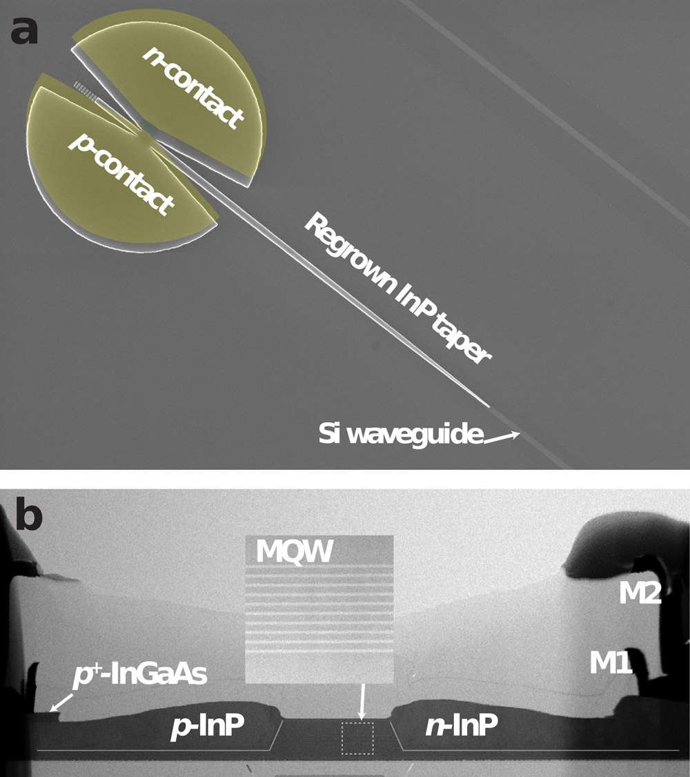
Figure 1: Fabricated III-V-on-Si membrane photodetectors on Si: (a) top-view scanning electron micrograph before metallization; (b) structural scanning transmission electron microscope cross section with inset close-up of InAlGaAs multiple QWs. Scale bar 500nm.
The photodetector mesas were formed using chlorine ICP-RIE and wet cleaning with hydrofluoric and sulfuric acid. The n- and p-type side-contact ‘butterfly’ regions were formed by selective-area regrowth of InP (Figure 1). The researchers comment that the thermal budget from these regrowth steps has been shown previously to be acceptable for bottom field-effect transistor (FET) performance preservation in fully depleted SOI devices with silicon germanium (SiGe) channels. Tin was used as n-type dopant, and zinc for p-type. The p-side included a zinc-doped InGaAs cap to improve the ohmic contact with the metallization.
The lateral current collection scheme decoupled the light propagation and carrier collection directions, enabling a strong optical confinement for ultra-compact devices with high efficiency. Simulations suggest that ballistic transport (i.e. minimal scattering) could occur in the wells, since the carriers don’t need to overshoot or tunnel through barriers.
The annealed metallization used a two-level CMOS-compatible process with molybdenum and tungsten plugs. The device geometry targeted “optimized absorption in the O-band, low dark currents and the ability to co-integrate light sources and modulators in the same platform”.
The optical contact with the underlying PIC also consisted of a regrown InP taper structure. The external quantum efficiency of the device was estimated to be as high as 69%. The capacitance was in the femtofarad range (femto=10-15). The researchers suggest that the benefits of ultra-small capacitances can only be realized with “devices monolithically integrated with CMOS electronics”. The dark current was also minimal, at sub-nA levels.
The researchers tested the response of 2μm-long photodetectors with stripe width of 200nm and 300nm. A 300nm-wide device had a 3dB bandwidth (f_{3db}) of 8.5GHz, compared with 1.5GHz for a similar device with straight contact (Figure 2).
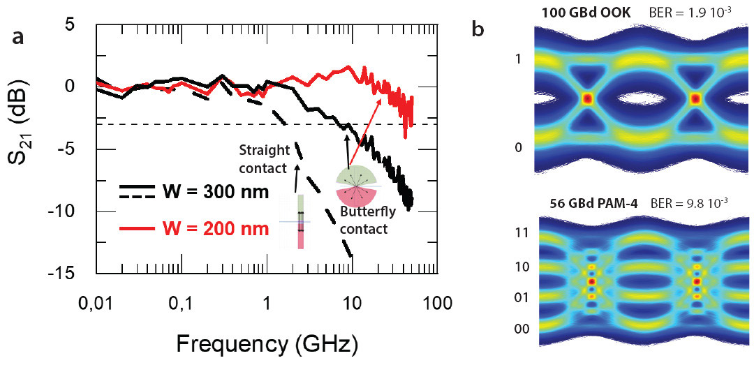
Figure 2: (a) Frequency response with varying stripe width, with (solid line) and without (dashed line) butterfly-shaped contacts. (b) Data reception at 100GBd OOK and 56GBd PAM-4 with corresponding bit-error-rates.
The 200nm device was tested under 100GBd on-off key (OOK) signal modulation of 1295nm light. The electro-optic bandwidth was around 65GHz. The researchers believe that adapting the device geometry could increase the bandwidth to 100GHz. The pad parasitics would need to be reduced to achieve this.
The team also performed 100Gbit/s pseudo random bit sequence OOK testing, demonstrating bit-error rates (BERs) of 1.9x10⁻³ with digital interpolation. “The eye opening in this experiment enables the use of multi-level modulation formats, allowing higher capacity per channel,” the team comments. They add: “As a practical example, we also show the eye diagram of a 112Gbit/s four-level pulse-amplitude modulation (PAM-4) signal with a calculated BER of 9.8x10⁻³, which has been recorded by a real-time oscilloscope” (Figure 2b).
https://doi.org/10.1364/OE.414013
The author Mike Cooke is a freelance technology journalist who has worked in the semiconductor and advanced technology sectors since 1997.


