


News: Optoelectronics
7 January 2021
GaInAsSb 1.55μm telecom device
ETH Zurich in Switzerland has demonstrated the first use of gallium indium arsenide antimonide (GaInAsSb) as an absorber material for 1.55μm telecom wavelengths [Akshay M. Arabhavi, Journal of Lightwave Technology, published online 9 December 2020]. The material was deployed in uni-traveling carrier photodiodes (UTC-PDs), which demonstrated enhanced response to modulated signals with a transit-limited bandwidth of 274GHz, compared with 107GHz for uniform GaAsSb absorbers. GaAsSb performance can be improved by grading the material to give 184GHz bandwidth, but clearly this still falls short of 274GHz.
Previously, it had been thought that the use of quaternary GaInAsSb absorber would not yield much benefit since the alloy components have similar bandgaps. The researchers attribute the GaInAsSb enhancement to improved electron transport in the fabricated devices. The UTC structure depends only on fast electron transport, an advantage over PIN diodes, which are limited by the slower hole drift movement through sections of the conventional structure.
Research leader Colombo Bolognesi comments that the ETH device “provides a nearly 3x improvement in ultimate speed over GaAsSb absorbers (also demonstrated by my group in 2005), and comparisons to similar InGaAs-based devices suggest that the quaternary GaInAsSb alloy is between 30 to 40% superior to InGaAs (the industry workhorse) despite being doped 6.5x higher than the InGaAs devices used for comparison.” He adds: “It is not everyday that a new material unexpectedly shows up with so much promise. We’ll keep at it and see where it goes.”
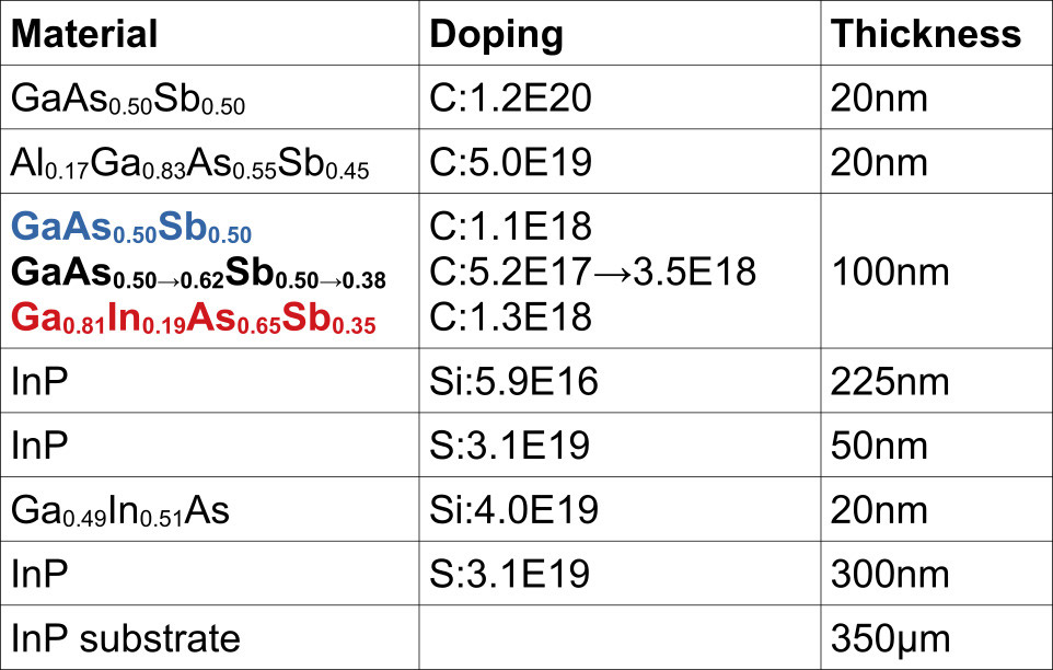
Table 1: Epitaxial material.
The semiconductor material (Table 1) for the UTC-PDs was grown by metal-organic vapor phase epitaxy on 2-inch semi-insulating (100) indium phosphide (InP) substrate. The structure was ‘type II’, where the heterojunction conduction and valence band steps go in the same direction.
The photodiodes (Figure 1) were formed by depositing a palladium/nickel/platinum/gold ohmic electrode as the ohmic p-contact, followed by wet etch of the absorber/collector mesa structure, titanium/platinum/gold metallization for the n-contact, and isolation mesa wet etch. 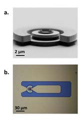 Co-planar waveguide probe pads were added after a Teflon-based etch-back planarization process.An anti-reflection coating consisted of silicon nitride.
Figure 1: (a) Scanning electron micrograph of UTC-PD following isolation mesa formation; (b) top-view microscope image of completed device with coplanar waveguide probe pads.
The resulting devices demonstrated a dark current of less than 10nA up to reverse biasing of up to 5V. The frequency performance was measured in the range 0.2-60GHz. The input light was a modulated 2mW signal at 1550nm wavelength delivered via lensed optical fiber with a 3μm spot diameter.
The 3dB cut-off frequency (f3dB) point was more than the measured 60GHz when the device areas were less than 80μm2. Removing the effect of the resistance-capacitance (RC) delay, the researchers extrapolated a transit-time-limited cutoff frequency (fT) of 274GHz for an 80μm2 area device (Figure 2). This value compares with 107GHz and 184GHz for GaAsSb absorber layer devices with uniform and graded compositions.
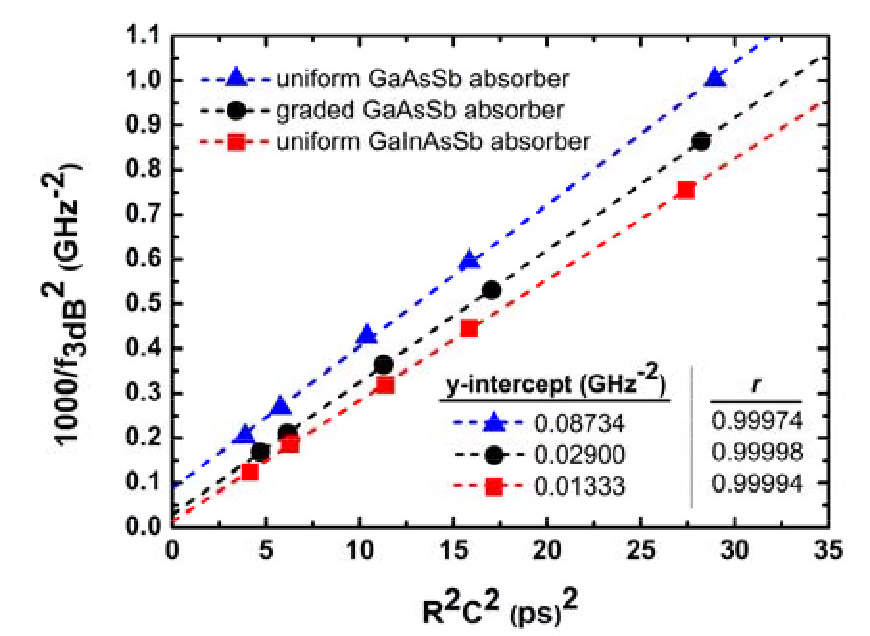
Figure 2: 1000/f23dB versus R2C2 for UTC-PDs with three different absorbers. Linear extrapolation to RC = 0 determines transit-limited bandwidth via the y-intercept value. The linear correlation coefficient r also shown.
At present, the performance-limiting factor is RC delay, which can be reduced with the size of the devices. Also, the GaInAsSb quaternary absorber was found to be 34% more responsive to light stimulation relative to the ternary GaAsSb (0.094A/W versus 0.070A/W).
The team comments: “The higher responsivity of GaInAsSb absorbers can be attributed to: (i) the narrower bandgap in Ga0.81In0.19As0.65Sb0.35 compared to GaAsSb; (ii) reduced carrier recombination in the absorber thanks to a reduced transit time; (iii) a relatively lower population of electrons in the absorber L-valley (reduced blocking to InP); and (iv) a longer Auger recombination lifetime of in GaInAsSb relative to GaAsSb”.
The indirect L-valley separation from the direct Γ-valley, which responds much more effectively to light, is thought to be larger in GaInAsSb relative to GaAsSb, resulting in lower electron population in the performance-sapping L-valley. In fact, GaAs and GaSb have separations of 0.284eV and 0.026eV, respectively, while the corresponding InAs and InSb separations are much larger: 0.716eV and 0.695eV. In addition, the L-valley has a much lower electron mobility.
The researchers hope to “improve the overall responsivity with resonant cavity structures and/or conversion to a waveguide architecture”. They add: “Significant improvements in responsivity are expected since optical electromagnetic simulations for the present UTC-PD demonstrators show that the peak optical field region is not aligned with the absorber layers.”
https://doi.org/10.1109/JLT.2020.3043537
The author Mike Cooke is a freelance technology journalist who has worked in the semiconductor and advanced technology sectors since 1997.


