


News: Markets
28 September 2020
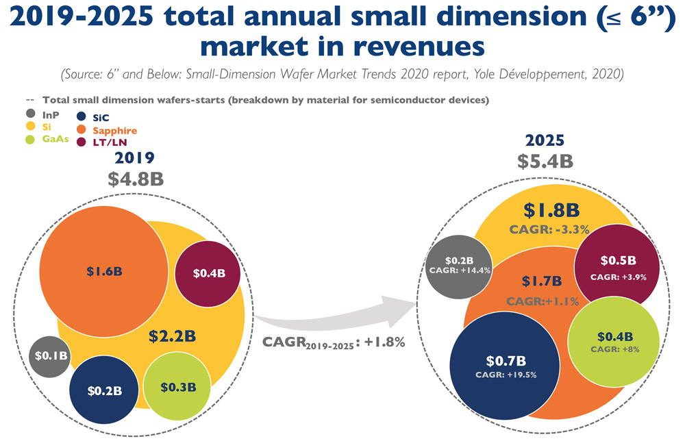
Small-wafer market growing at 1.8% CAGR to $5.4bn in 2025.
“The small-wafer (1”–6’’) market is anything but ‘dead’,” asserts Gaël Giusti PhD, technology & market analyst specializing in Semiconductor Manufacturing and Equipment & Materials at market research & strategy consulting firm Yole Développement in the report ‘6” and Below: Small-Dimension Wafer Market Trends’, which forecasts a compound annual growth rate (CAGR) of 1.8% over 2019–2025 to $5.4bn (despite falling from 63% to 53% of the total wafer market in terms of units).
‘More than Moore’ applications represent the overwhelming part of this market, which is hence still very dynamic. In fact, non-silicon wafer markets exhibit moderate to strong CAGRs over 2019-2025: e.g. 19.5% CAGR to $712m in 2025 for silicon carbide (SiC). In the 6”-and-below market, only silicon exhibits a moderate negative CAGR, with –3.3% for sub-6” wafers, due mostly to power & RF applications increasingly transitioning to 8” and even 12” diameters.
According to Yole, the sub-6” market strength can be attributed to a ‘good enough’ ratio of device performance/fabrication cost-per-die, so that large capital expenditure (CapEx) and risky process changes cannot always be fully justified. “This ‘good enough’ concept is important and is a strong driver in the use of small-dimension wafers,” says Vishnu Kumaresan PhD, technology & market analyst, Semiconductor Manufacturing.
In parallel, Yole notes strong market drivers for each materials and related applications.
For example, SiC for power electronics applications is currently seeing huge investment, with almost all leading power electronics and compound semiconductor companies deeply involved in the development of SiC-based solutions.
“In the 2019-2020 period, there has been significant news on SiC device and module business in terms of partnerships and acquisitions,” says Ezgi Dogmus PhD, technology & market analyst, Compound Semiconductor & Emerging Materials. “This clearly validates SiC substrate and device manufacturers’ desire to climb up the value chain to benefit from growing business opportunities at the module level,” she adds.
Indium phosphide (InP) and datacom applications also represent a good example to highlight the added value of small-dimension wafers. In fact, driven by indium phosphide (InP) – as well as gallium nitride (GaN) bulk wafers – the 2” market is forecasted to grow (in units) the most rapidly of all sub-6” wafer sizes.
This is followed by a robust 6” market (with a compound annual growth rate (CAGR) of 2.9% over 2019-2025): the growth of the 6” wafer markets will be mostly driven by gallium arsenide (GaAs), silicon carbide (SiC) wafers and sapphire (should micro-LEDs fully emerge).
The case of sapphire is particularly interesting, since the competitive landscape has changed tremendously after a price collapse, with only a handful of players serving a high-volume yet saturated LED market, notes Yole. However, the micro-LED market could boost demand significantly by 2023, especially in the 6” range, it adds. “Micro-LEDs could also propel the gallium arsenide (GaAs) wafer market, particularly for red pixels,” says Ahmed Ben Slimane PhD, technology & market analyst, Compound Semiconductors. “Indeed, the GaAs growth is significantly boosted by photonics applications, with GaAs vertical-cavity surface-emitting laser (VCSEL) technology strongly dominating this market due to the high volume demand for consumer 3D sensing applications, causing GaAs to grow with a CAGR of no less than 8% between 2019 and 2025,” he adds. “Overall, new applications and needs are driving evolutions in wafer diameters, by material and by application”. The GaAs market is also studied in Yole’s ‘Compound Semiconductor Quarterly Market Monitor’ for Q3/2020.
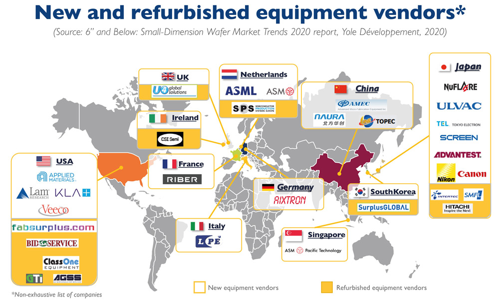
In parallel to mainstream semiconductor equipment there is a vibrant market for refurbished equipment and maintenance, notes the report ‘6” and Below: Small-Dimension Wafer Market Trends’. Almost all major equipment vendors, in terms of 2019 revenue, have sub-8” solutions, in the form of either new or refurbished equipment. “This is significant and connected to the ‘fabs never die’ trend,” comments Giusti.
Less well known is the existence of a market for depreciated fabs, which also represent tremendous opportunities to produce devices at low cost for any volume. For example, there is still significant demand for 6” silicon wafers in standard power IGBT (insulated-gate bipolar transistor) and MOSFET (metal-oxide-semiconductor field-effect transistor) devices. Higher-end devices can then be fabricated in brand-new fabs, for example Robert Bosch and Infineon Technologies in the power electronics industry, in the silicon 300mm range, which is also a way to secure future supplies and assert one’s dominance in the market, reckons Yole.
“A similar trend is at play in the SiC wafer manufacturing industry, with some major players moving quickly to 8” wafer diameter and securing their supply chain while leaving behind 6” (and even more so 4”) wafer processing capacities,” notes Kumaresan. “With the increased use of non-silicon substrates, more and more players are offering specific processing equipment for a given material and/or are proposing equipment which can adapt to different materials and diameters, including 4” and 6”,” he adds. “This equipment can be astutely used in fully depreciated sub-6” silicon wafer fabs, creating opportunities for players small and large to offer a highly competitive device fabrication cost,” he concludes.
GaAs substrates SiC substrates


