


News: LEDs
11 September 2020
Green and orange LEDs on porous GaN
University of California Santa Barbara (UCSB) in the USA has been using a gallium nitride porosification process to increase the wavelength of indium gallium nitride (InGaN) micron-scale light-emitting diodes (μLEDs) [Shubhra S. Pasayat et al, Appl. Phys. Lett., vol117, p061105, 2020]. The porous GaN is less rigid, allowing overlying InGaN ‘pseudo-substrate’ (PS) layers to be less strained.
The relaxed InGaN in turn increases indium uptake during regrowth processes through the ‘composition pulling effect’, creating higher-indium-content layers and hence longer emission wavelengths. Composition pulling is ascribed to the reduced lattice mismatch between the InGaN growth front and the underlying InGaN pseudo-substrate, compared with InGaN grown directly on GaN. The work resulted in green (500-565nm)- and even orange (590-625nm)-emitting devices.
The researchers see the potential for applications from near-eye head-mounted to large-area self-emitting displays. Also, smaller device sizes often allow for faster switching speeds for GHz-level modulation bandwidth in visible light communications (VLC). “Owing to their small form factors, μLEDs are also being considered to possess immense potential in medical applications and mask-free lithography,” the team adds.
The UCSB group has also recently reported on use of the same concept for producing high-aluminium-content AlGaN pseudo-substrate films, which may lead to better-performing very-short-wavelength deep-ultraviolet-emitting devices [Shubhra S. Pasayat et al, Appl. Phys. Lett., vol117, p062102, 2020].
For the InGaN μLEDs, the UCSB team performed metal-organic chemical vapor deposition (MOCVD) on c-plane sapphire. The GaN layers used trimethyl-gallium as the metal precursor, while for InGaN triethyl-gallium and trimethyl-indium were used. The nitrogen source was ammonia. Silicon doping for n-type conductivity came from disilane (Si2H6).
The first steps consisted of growing 2.8μm of unintentionally doped (UID) GaN buffer, followed by 800nm of 5x10¹⁸/cm3 Si-doped GaN (GaN:Si) and a 100nm UID GaN cap.
A 2mmx2mm die from the material was dry etched into square tiles with dimensions from 8μmx8μm up to 20μmx20μm. The target etch depth was 550nm. Electrochemical (EC) etching porosified the GaN:Si layer. Some parts of the die were protected from the electrochemical process to allow the growth of reference InGaN material. The electrochemical etch used a metal contact on the exposed GaN:Si layer as the anode, a platinum cathode, and 0.3M oxalic acid electrolyte.
The porous material was subjected to MOCVD regrowth, producing LED structures (Figure 1): 180nm of InxGa1-xN:Si, 10nm of unintentionally doped GaN, a multiple quantum well (MQW), 120nm of magnesium-doped In0.04Ga0.96N:Mg, and 16nm of heavily doped p++ n0.04Ga0.96N:Mg. The x-parameter for the 180nm InGaN layer was either 4% or 9% In.
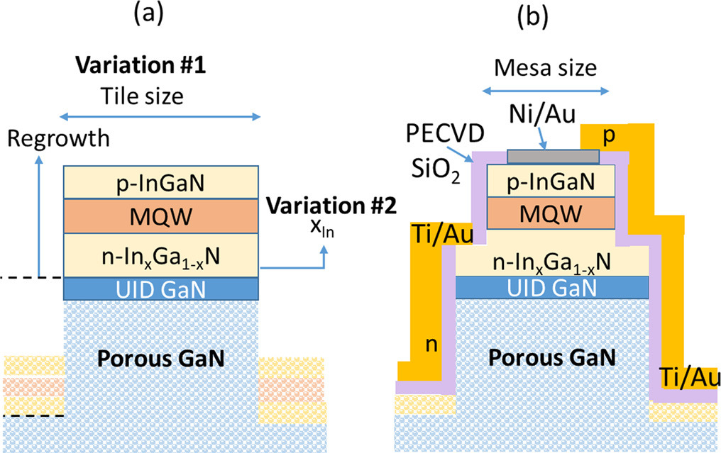
Figure 1: Cross-sectional schematic of regrown green micro-LED structure (a) and (b) post-fabrication.
The MQW consisted of three 3nm nominal In0.2Ga0.8N wells capped with 2nm of aluminium gallium nitride (Al0.1Ga0.9N), and 10nm of UID GaN. The p-type Mg-doped layers were grown on the last well of the sequence.
The LED structure was fabricated with reactive ion etch isolation of the structure, followed by plasma-enhanced chemical vapor deposition (PECVD) of silicon dioxide insulation. Contacts were formed using wet etch and deposition of nickel/gold p-contacts and titanium/gold n-contacts. The researchers point out that the LED fabrication was “basic”, and that many enhancements could improve light output performance.
The team first looked at the mean wavelength of the electroluminescence (EL) from 4μmx4μm-area LEDs on tiles of various dimensions with a base InGaN layer of 4% indium content (Figure 2). As the tiles became smaller, the wavelength red-shifted: with 10A/cm2 injection current density the wavelength for 20μmx20μm tiles was 525nm, while 8μmx8μm-tile μLEDs produced 561nm radiation. The researchers estimated the indium content to be 0.22 and 0.245, respectively. A μLED on the non-porous region of the die emitted at an even shorter wavelength of 497nm, giving an estimated indium content of 0.2, the target value for the growth process.
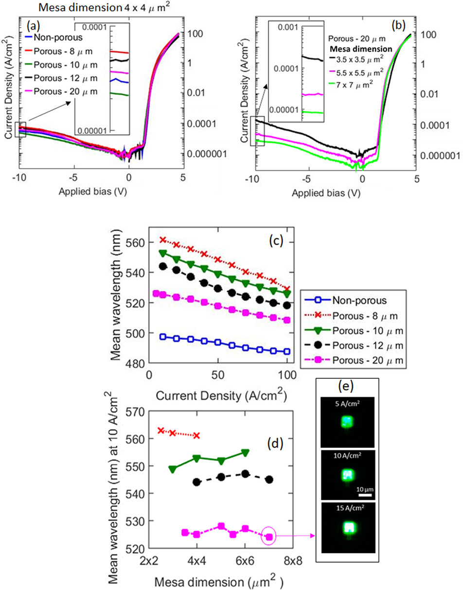
Figure 2: Current–voltage characteristics of (a) 4μmx4μm mesa μLEDs fabricated on various-sized tiles and on unpatterned non-porous material, and (b) for various-sized mesa /microLEDs fabricated on 20μm tiles. (c) Mean EL wavelength dependent on current density, for 4μmx4μm mesa μLEDs fabricated on various-sized tiles and on unpatterned non-porous region. (d) Mean EL wavelength dependent on device dimensions fabricated on various-sized tiles at 10A/cm2 injection. (e) EL images of 7μmx7μm μLED on 20μm tile at varied current injection.
The researchers explain: “The higher degree of relaxation in the n-InGaN layer on smaller tiles resulted in a higher n-InGaN in-plane lattice constant and led to an increased indium uptake during the growth of the InGaN MQW active region of the LEDs due to the composition pulling effect, resulting in the red-shift of the EL peak.”
The turn-on voltages were in the range 3-3.5V for reasons that are not yet well understood. One would hope that longer-wavelength devices would have a lower turn-on voltage, reflecting the narrower bandgap. Lower turn-on voltages are an important factor in power efficiency.
The emission wavelengths were largely independent of the size of the μ LED mesa, showing no clear trends. The researchers believe this indicates uniform indium incorporation across the tiles.
The external quantum efficiency (EQE) of the devices was less than 0.44% at 100A/cm2, with the largest values being from the largest μLEDs on the 20μm tiles. The light was only measured on the sapphire side of the device within an approximate 60° half-angle exit cone. “This geometry was preferred over the measurement of packaged devices in an integrating sphere as it more accurately imitated how micro-LEDs are used in displays,” the team writes.
The better efficiency of the larger μLEDs suggests losses from the perimeter of the active area through surface recombination effects. The team comments: “Etched surfaces are known to possess crystallographic defects, impurities, nitrogen vacancies, and dangling bonds that can introduce trap states within the bandgap, which can act as non-radiative recombination centers.”
Another effect was a blue-shift with increasing current, particularly in devices on the smaller tiles. The researchers comment: “As the indium incorporation in the InGaN wells of the MQW active region increased with decreasing tile size, the barriers of the MQWs were still composed of AlGaN and GaN, giving rise to higher piezo-electric fields in the LED active region and, hence, a higher quantum-confined Stark effect (QCSE). This blue-shift can be lowered by using InGaN as barrier material in the MQWs.”
Using a 9% indium-content 180nm InGaN base layer reduced the turn-on voltage to around 2V at the cost of up to three orders of magnitude increased reverse-bias leakage. The EL wavelength was 616nm, ‘orange’, at 60A/cm2, while the EQE was around 0.001% at 100A/cm2. The estimated indium content in the wells was 0.3. A comparison device with a 4%-indium base layer had an emission wavelength of 536nm at 60A/cm2.
The team reports: “Compared to the green-emitting μLEDs, as the indium composition increased in the n-InxGa1-xN base layer as well as the quantum well for the orange-emitting μLED, enhanced v-defect formation led to the introduction of a lot of leakage pathways. This led to an enhanced leakage current in the orange μLED.”
Although the EQE of the orange-emitting device was pitifully low, the researchers believe it “demonstrates the potential of this technology for the fabrication of strain-relaxed color-tunable μLEDs.”
InGaN InGaN pseudo-substrate Green LEDs Orange LEDs
https://doi.org/10.1063/5.0011203
https://doi.org/10.1063/5.0017948
The author Mike Cooke is a freelance technology journalist who has worked in the semiconductor and advanced technology sectors since 1997.


