


News: Optoelectronics
24 September 2020
InAs quantum dot laser diodes on SOI
Researchers based in China claim the first electrically pumped indium arsenide quantum dot in gallium arsenide matrix (InAs/GaAs QD) narrow-ridge Fabry-Perot (FP) lasers on silicon-on-insulator (SOI) substrates [Wen-Qi Wei et al, Optics Express, vol28, p26555, 2020].
The team from Beijing National Laboratory for Condensed Matter Physics, University of Chinese Academy of Science, and Songshan Lake Materials Laboratory, hope to contribute to the development of monolithic integration of III-V laser sources into silicon photonics integrated circuit (Si PIC) chips.
The researchers comment: “Integration of III-V materials on Si combines the superior optoelectronic properties of III-V materials and the compatibility with currently mature manufacturing processes offered by CMOS foundries.” They add: “Overall, the realization of electrically pumped III-V FP lasers on SOI will enable the great potential integration opportunity for on-chip silicon photonic telecom transmitters.”
In future work, the team hopes to develop direct butt coupling into SOI-based silicon waveguides through selective-area growth of InAs/GaAs QD lasers inside SOI templates with pre-patterned trenches.
The material was grown by molecular beam epitaxy (MBE) in two systems – one for silicon and the other for III-V growth. The 8-inch-diameter SOI substrate consisted of 3μm buried oxide (BOX) insulator (SiO2) and 340nm silicon top layer patterned with U-shape trenches in the [110] direction of the silicon crystal structure.
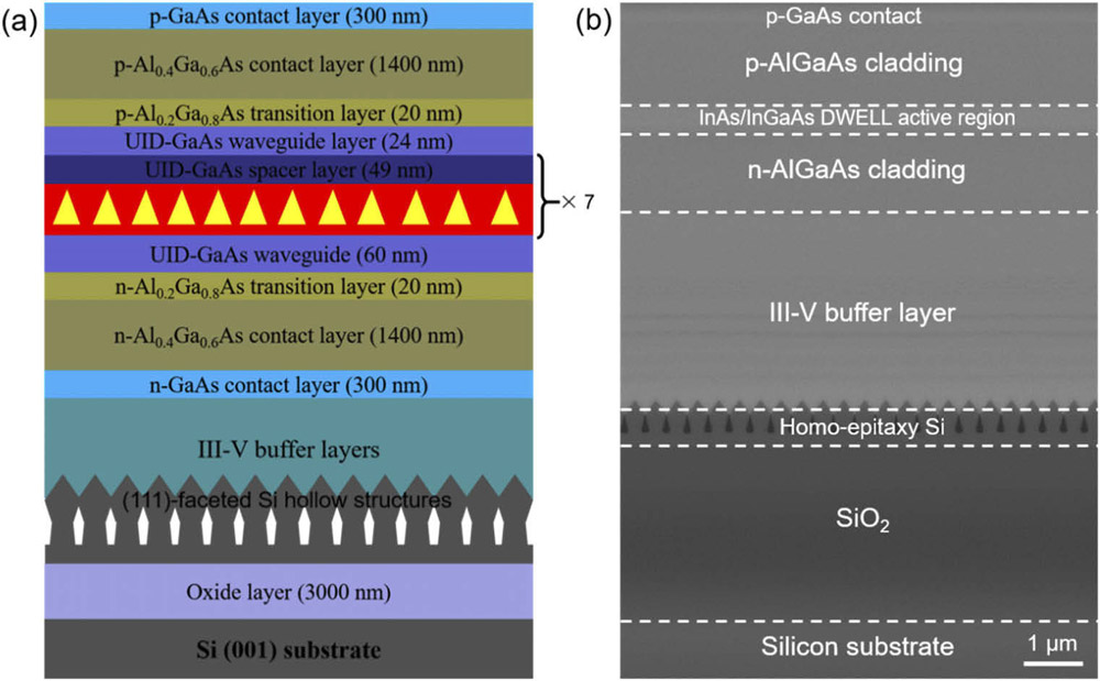
Figure 1: Schematic (a) and scanning electron microscope image (b) cross sections of InAs QD laser structure on SOI substrate.
The substrate was diced into 3.2cmx3.2cm pieces and deoxidized in dilute hydrofluoric acid. The first MBE process consisted of 420nm of silicon at 600°C, resulting in a coalesced sawtooth surface with {111} facets on voids over the U-shaped trenches (Figure 1).
The III-V buffer structure was grown at two temperatures – 380°C for a 40nm nucleation layer and 540°C for the main material. The nucleation layers consisted of 10nm AlAs and 30nm GaAs. This was followed by 360nm of high-temperature GaAs and a series of InGaAs/GaAs and InAlAs/GaAs strained-layer superlattices (SLSs) to filter out threading dislocations to a level of 9.6x10⁶/cm2.
The active region of the laser consisted of seven layers of InAs QDs in a GaAs matrix, forming a dot-in-well (DWELL) structure. The DWELL was grown at 430°C, while the surrounding cladding and contact layers were grown at 580°C and 540°C, respectively. In photoluminescence spectra, the wavelength peak occurred at 1298nm. A comparison structure grown on GaAs substrate had a peak at 1275nm, the difference being attributed to “substrate temperature variation”.
Narrow-ridge lasers were fabricated parallel and perpendicular to the underlying v-groove structures. Dry and wet etch were carried out to achieve smooth sidewalls of the ridges and mesas. The top ridge mesa reached down to about 100nm above the active region.
The contacts were annealed nickel-germanium-gold/gold and titanium/platinum/titanium/gold for the n- and p-sides, respectively. The substrate was thinned to 100μm thickness before cleaving into laser bars. The cleaved mirror facets were not coated with anti-reflective layers.
The threshold for continuous wave (CW) operation of a 4μmx1mm bar was 140mA at 0°C, increasing to 175mA at 5°C and 10°C.
The threshold was reduced to around 50mA for the 0-10°C temperature range in 100ns pulsed operation with 5% duty cycle, allowing heat dissipation and therefore avoiding thermal degradation of performance. As the temperature increased to 60°C, the threshold increased to 90mA for pulsed injection.
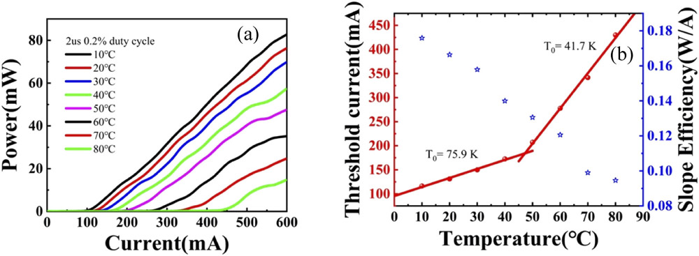
Figure 2: (a) Temperature-dependent light output power-current characteristics of InAs/GaAs QD laser under pulsed operation. (b) Threshold current and slope efficiency versus temperature.
For CW performance, the heat build-up was largely attributable to the thermally insulating nature of the SiO2 component of the SOI substrate.
The output powers in pulsed mode was less than 5mW at 200mA injection. For 0°C CW operation, the output power was just over 4mW at the same current. The maximum output power reached in pulsed mode was 6.5mW at 240mA.
The team hopes that high-reflection coatings and facet passivation could improve output power and lower thresholds.
The characteristic temperature T0, reflecting changes in threshold current, was 184.2K below 30°C, reducing to 58.1K above that due to heat dissipation problems. The 184.1K value was higher than for previously reported 1.3μm and 1.5μm QD Fabry-Perot lasers grown on silicon substrates.
The slope efficiency of the device is described as “poor” at 0.034W/A at room temperature (20°C). The researchers suggest that “high internal loss, resulting from high doping level in the AlGaAs cladding layers” was to blame for this.
The laser emissions were multi-mode, with the main peak just above threshold being from the 2nd excited state with a wavelength of 1210nm. As the current injection increased to 130mA, the 1st excited state peak at 1240nm rose in strength.
Operation with 2μs pulses at 0.2% duty cycle enabled increased temperature operation at 80°C, but with increased threshold of 130mA at room temperature. The maximum room-temperature output power was 75mW under these conditions. In the 0-40°C range, T0 was 75.9K, reducing to 41.7K for 40-80°C.
The researchers see thermal dissipation as being the main barrier to progress. The team comments: “By implementing thick metal contacts with externally bonded heat-sink such as thermal shunt design, it would significantly help reducing the heat accumulation inside the laser chips, which could strongly contribute to better device performance. Ultimately, by selectively growing III-V lasers on the bottom silicon of SOI substrate, the generated heat from laser devices could be effectively dissipated into the substrate, rather than isolated by the BOX layer.”
Another possibility for improved thermal dissipation, mentioned by the team, is selective-area growth of InAs QD lasers within the SOI trenches, allowing heat transfer to the more conductive silicon substrate.
InAs/GaAs QD Fabry-Perot laser SOI substrates InAs GaAs
https://doi.org/10.1364/OE.402174
The author Mike Cooke is a freelance technology journalist who has worked in the semiconductor and advanced technology sectors since 1997.


