


News: Microelectronics
29 October 2020
Optimizing SiC MOSFET performance
Two researchers at the State University of New York Polytechnic Institute (SUNY Poly) in the USA claim record-breaking performance for 4H-polytype silicon carbide (SiC) lateral metal-oxide-semiconductor field-effect transistors (MOSFETs) [Nick Yun and Woongje Sung, IEEE Transactions On Electron Devices, published online 14 October 2020]. In particular, a 0.3μm-channel device with 2.5μm gate-drain spacing achieved 7.7mΩ-cm2 specific on-resistance and 450V breakdown.
SiC-based devices are looking to supplant the more mature silicon technology for power integrated circuit applications, based on a larger 3MV/cm critical electric field for breakdown, an order of magnitude larger than for silicon. A challenge for SiC-based devices has been to achieve low on-resistances combined with high breakdown voltages.
Yun and Sung’s work was partially supported by the US Office of Energy Efficiency and Renewable Energy (EERE), Department of Energy, with North Carolina State University’s Power America Institute.
Yun and Sung designed a wide range of MOSFETs (Figure 1), using varied dimensions. The devices were fabricated under a range of process conditions at the X-FAB 6-inch wafer foundry in the USA. The substrate featured a 6μm heavily-doped n+ drift layer.
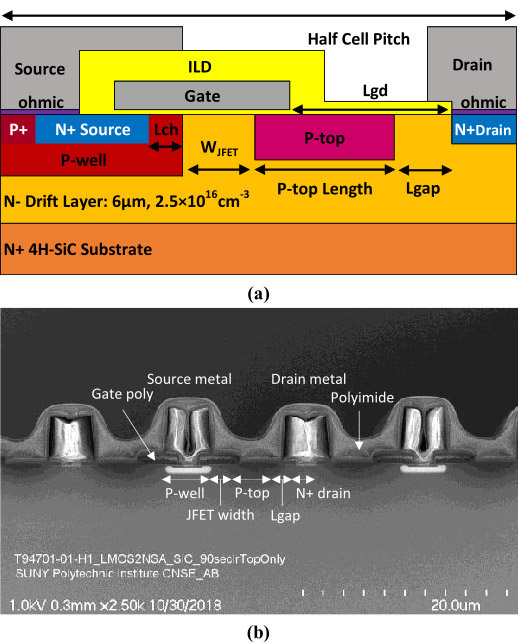
Figure 1: (a) Schematic and (b) scanning electron microscope cross-sectional view of fabricated 600V 4H-SiC lateral MOSFET.
Aluminium ion implantation was used for the various p-type regions. The p-top region formed a single reduced surface field (RESURF) structure. Combined with the p+ body region, the p-top region made up concentric floating field ring and junction-termination-extension (JTE) structures for hybrid-JTE edge termination. The p-well enabled accumulation- and inversion-mode channels to be realized. The accumulation mode generally resulted in lower specific on-resistance (RON,sp).
High-temperature nitrogen ion implants created the n+ source and channel-stop regions. The doping was activated with a 10-minute anneal at 1650°C, under a carbon cap.
The gate insulation was achieved using 1175°C dry oxidation and annealing in nitric oxide (NO). After the gate oxide was patterned, the interlayer dielectric (ILD) was applied. Nickel was then used to give a self-aligned silicide transistor formation process. This was followed by rapid thermal annealing (RTA) at 900°C or 1000°C. The higher temperature resulted in lower contact resistance.
The device fabrication was completed by 4μm aluminium deposition for the source contact and gate pad, and nitride/polyimide front-side passivation.
The lateral layout of the device consisted of multiple interdigitated fingers in source- or drain-centered formats (Figure 2). The source-centered layout did not require edge-termination, while the drain-centered transistors needed such structures to “alleviate crowding of electric fields at P+ regions in the periphery and extend the horizontal depletion layer to achieve the specified breakdown voltage of the device”.
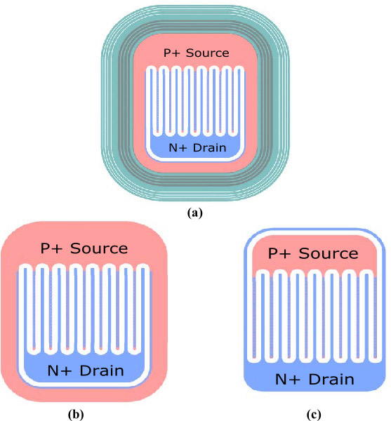
Figure 2: Simplified topological view of drain-centered layout methodology with (a) and without (b) edge termination, and (c) source-centered layout methodology for designing lateral MOSFETs. Gate pad not shown.
The source-centered approach achieved a 100μA blocking voltage of 600V without edge-termination. By contrast, such blocking was limited to 280V in drain-centered devices. Even worse 180V blocking behavior was seen in devices without p-top RESURF structures, regardless of layout. Edge-termination in the drain-centered MOSFETs enabled comparable 600V blocking to the source-centered device.
The on-resistance of the device decreased at high temperature, compared with room temperature (25°C). The minimum came at 125°C, but on-resistance continued to be lower than at room temperature in the range up to 200°C. Yun and Sung note: “The increase of RON,sp from 125°C and onward could be due to the governance of other resistances at high temperatures such as JFET, contact, metal, and drift resistance”
Generally, the devices had a 5μm gate-drain distance. A source-centered device with smaller 2.5μm gate-drain spacing, and 0.3μm-channel length, still achieved a reasonable 450V breakdown voltage, along with the lowest 7.7mΩ-cm2 RON,sp. The 450V corresponds to 180V/μm blocking, compared with 120V/μm for the 5μm gate-drain devices (0.5μm channel).
https://doi.org/10.1109/TED.2020.3027652
The author Mike Cooke is a freelance technology journalist who has worked in the semiconductor and advanced technology sectors since 1997.


