


News: Optoelectronics
2 October 2020
Simultaneous emission-detection
Researchers in China and Japan have been exploring the simultaneous emission-detection capabilities of multiple quantum well (MQW) III-nitride diode arrays [Yongjin Wang et al, Applied Physics Express, accepted manuscript online 11 September 2020]. The hope of the team from Nanjing University of Posts and Telecommunications and Zhengzhou University in China and Nagoya University in Japan is to develop advanced monolithic III-nitride information systems for Internet of Things (IoT) deployment, based on such multi-function devices.
III-nitride diodes have the capability to both emit and detect light. The researchers have successfully combined these capabilities, performing these functions at the same time.
The team comments: “By integrating with programmed circuits, multi-functioning MQW-diodes open up feasible routes toward a wide range of exciting applications from automatic brightness control to touchless shared user terminals and simultaneous illumination-imaging system. In particular, the shared user terminals communicate with each other via light and thus provide non-contact reader/writer interfaces, offering protective actions to avoid the cross-contamination due to touch with conventional handwritten terminals and to help prevent the spread of viruses. These monolithically integrated devices benefit from the simplicity of a single growth and fabrication process, and this integrated on-chip system could produce better performance with advances in the material growth and device fabrication.”
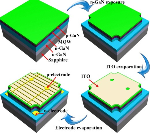
Figure 1: Fabrication process flow of MQW-diode array.
The MQW-diode arrays were fabricated using 2inch-diameter III-nitride on sapphire material (Figure 1). The n-type gallium nitride (n-GaN) contact layer was exposed using inductively coupled plasma reactive-ion etch to a depth of 750nm. Indium tin oxide (ITO) transparent conductor material was applied onto the p-GaN contact layer through evaporation techniques, and then annealed. A lift-off process was used to deposit and pattern the chromium/platinum/gold metal used for the n- and p-electrodes.
The devices in 4x4 arrays were electrically isolated by trenches filled with 230nm-thick silicon dioxide insulation. Bonding pads and metal lines were formed from titanium/platinum/gold. The individual MQW-diodes measured 1mmx1mm.
The electroluminescence peak at 442nm wavelength had a 36nm overlap with the tail of the photoresponse spectrum (Figure 2). Communication between two array elements achieved a 2k bit per second rate with pseudorandom binary sequence (PRBS) modulation. The peak-to-trough voltage difference for the binary pulse modulation was 1.6V. The detected signals were about 1.5mV high.
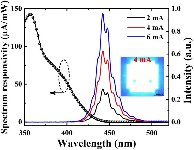
Figure 2: Measured EL and responsivity spectra, and inset emission at 4mA injection.
The researchers realized an automatic light brightness control setup where a 405nm laser pointer could issue a coded sequence of pulses that would be detected by the array, and then interpreted by control circuitry that would adjust the light output to the desired level, considering ambient light conditions through feedback.
Another demonstration involved using the array to recognize characters from images projected on the diodes with potential for a touchless-terminal application (Figure 3).
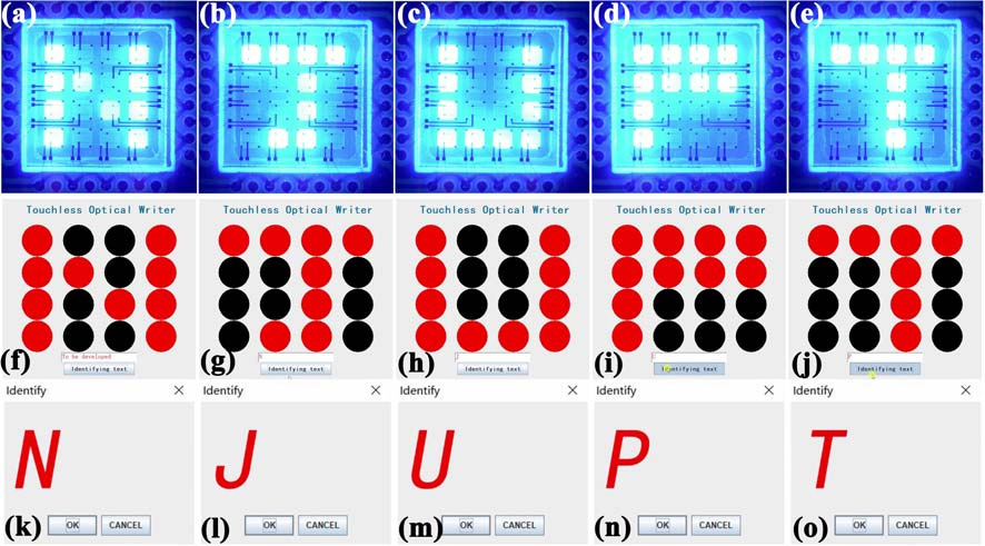
Figure 3: (a)-(e) Light-activated emission pattern; (f)-(j) Corresponding pattern displayed on user interface; (k)-(o) corresponding output character sequence.
The team is developing circuitry to effectively extract photocurrents while the devices are also simultaneously operating as LEDs. “We can envision that a large MQW-diode array can realize the simultaneous illumination-imaging system with improved performance,” the researchers comment. In their paper, they describe preliminary experiments demonstrating the potential of this with their 4x4 array combined with optical imaging and electronic/software processing systems.
Yongjin Wang reports: “The simultaneous illumination-imaging system has three operation modes: illumination, imaging, and a simultaneous illumination-imaging operation. It means the micro-LED screen can display and image at the same time.” He adds that changes in environmental light conditions creates a photocurrent inside the chip, allowing a feedback signal to control the operation.
https://doi.org/10.35848/1882-0786/abb786
The author Mike Cooke is a freelance technology journalist who has worked in the semiconductor and advanced technology sectors since 1997.


