


News: LEDs
12 November 2020
MOCVD tunnel junctions for GaN LEDs
University of California Santa Barbara (UCSB) in the USA claims the highest performance so far for tunnel-junction micron-sized blue light-emitting diodes (TJ μLEDs) grown by metal-organic chemical vapor deposition (MOCVD) [Panpan Li et al 2020 Semicond. Sci. Technol., vol35, p125023, 2020].
In particular, very low forward voltages (Vf) were achieved by enhancing the tunneling probability and the activation efficiency of the p-GaN layers by inserting an indium gallium nitride (InGaN) layer into the tunnel junction and by using a selective-area growth (SAG) process, respectively. The performance of the TJs is comparable to that from molecular beam epitaxy (MBE) growth processes, it is claimed.
The InGaN insertion layer uses a difference in charge polarization relative to GaN to introduce band-banding effects that reduce the tunneling distance, hence increasing the tunneling probability.
The researchers see their work as overcoming size limitations on TJ μLEDs, enabling low Vf even for larger μLEDs and for regular-size LEDs. MOCVD is a much preferred process over MBE in large-scale, high-output manufacturing contexts. “This work solves the key challenges of MOCVD-grown TJs,” the team adds.
Tunnel junctions are seen as an alternative to transparent conductive oxides (TCOs) like indium tin oxide (ITO) for improving current spreading and thus emission uniformity and efficiency in GaN-based LEDs. Unfortunately, up to now the increased Vf penalty has wiped out any potential benefit in terms of reduced light absorption.
Further, TJs could provide interconnections between stacked ‘cascaded LEDs’ of devices with different color emissions, possibly enabling a reduced complexity assembly process for blue/green/red LED displays. Other potential benefits could be seen for producing edge-emitting laser and vertical-cavity surface-emitting laser (VCSEL) diodes.
The researchers used commercial blue LED material on patterned sapphire substrate (PSS) as a template for the overgrowth of TJ structures. Solvents including aqua regia were used to clean the surface before the overgrowth of III-N materials by MOCVD. The layer structure (Figure 1) consisted of 3nm silicon-doped n-In0.15Ga0.85N, 20nm n+-GaN, 350nm n-GaN, and 15nm n-GaN cap. A sample without the InGaN interlayer was also produced for comparison. A further variation was a structure produced by SAG.
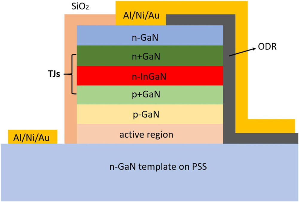
Figure 1: Schematic structure of InGaN TJ μLEDs.
The material was etched into square micro-LEDs of varying sizes from 10μm to 100μm sides before rapid thermal annealing for 30 minutes at 700°C to re-activate the p-type doping.
The SAG process involved the creation of silicon dioxide pillars – these were removed before the re-activation anneal. The team explains: “The apertures on the p-GaN surface by SAG create additional vertical out-diffusion paths for the hydrogen with a much shorter diffused distance than that to sidewall.”
Hydrogen is the main factor passivating the magnesium (Mg) acceptors that provide p-type doping in GaN. The researchers explain: “It is well known that decomposing the Mg–H complex in the p-GaN by thermal annealing and removing hydrogen atoms are the key points to activate the p-GaN.” While the presence of hydrogen is practically inevitable in processes involving organic compounds (e.g. MOCVD), MBE has an advantage here since recipes can be designed that avoid the element’s presence.
The LED fabrication involved reactive-ion etch with silicon tetrachloride to expose the n-GaN contact layer, ion-beam deposition of an omnidirectional reflector (ODR) constructed from silicon dioxide and tantalum pentoxide, sidewall passivation with 25nm silicon dioxide, and deposition of aluminium/nickel/gold metal contacts. Finally, the devices were diced, mounted on silver headers, and encapsulated in silicone.
The SAG and non-SAG devices with 3nm n-InGaN interlayer in the tunnel junction achieved similar, reasonably uniform light output intensity for devices up to 100μm. The paper does not contain images of the reference devices without InGaN, but the team reports: “We notice that the luminous images of the reference TJ μLEDs were not uniform with a brighter electrical luminous (EL) intensity at the edge and a darker EL intensity at the center area.” The researchers ascribe the improvement with InGaN interlayer to “higher tunneling probability at the InGaN TJs”.
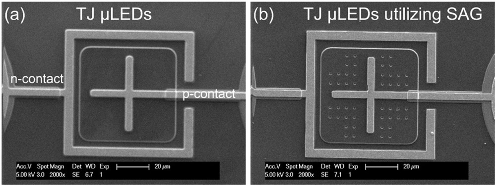
Figure 2: Scanning electron microscope images of fabricated 60 μmx60μm (a) InGaN TJ μLEDs and (b) SAG InGaN TJ μLEDs.
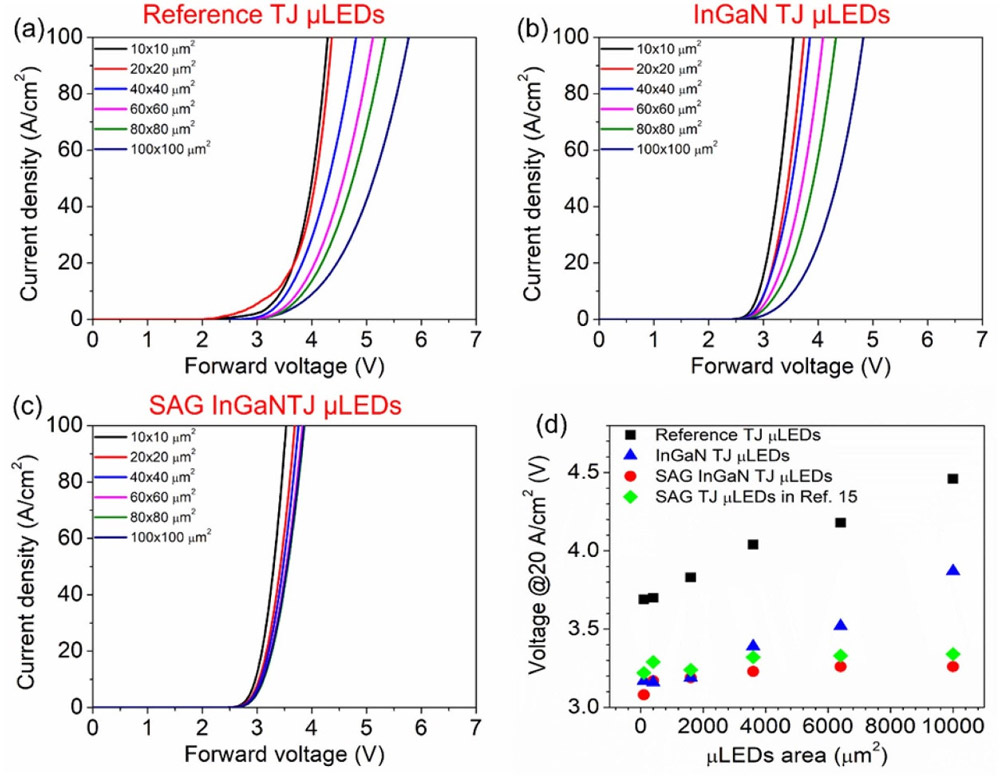
The difference between the InGaN TJ and the SAG InGaN TJ was revealed in the Vf performance, with the SAG process resulting in a lower value that is maintained up to dimensions of 100μm (Figure 3). A low Vf means that the input power is lower for a given current injection, increasing efficiency.
 f curves of μLEDs with sizes from 10μm to 100μm; (d) plot of Vf at 20A/cm2 as a function of size.">
Figure 3: (a)–(c) Current density–Vf curves of μLEDs with sizes from 10μm to 100μm; (d) plot of Vf at 20A/cm2 as a function of size.
The Vf at 20A/cm2 injection varied between 4.6V to 3.7V for the reference TJ LEDs without InGaN interlayer with sizes from 100μm to 10μm, respectively. The higher Vf in the larger devices is explained by the increased difficulty in hydrogen escaping from the p-GaN layers during the annealing activation process. The corresponding voltages for the InGaN TJ devices were 3.86V and 3.16V. The enhanced tunneling probability with InGaN interlayer increased the current flow for a given potential.
There was a much smaller variation between 3.08V and 3.25V for the SAG InGaN TJ. The enhanced out-diffusion of hydrogen through the SAG apertures explains the improved performance. These values are 0.1-0.2V lower than for SAG TJs produced without InGaN interlayer reported earlier this year by UCSB.
The team comments: “We note that the Vf of the μLEDs with ITO contact from the same epitaxy wafer is varied from 2.93V to 2.97V and independent on the sizes.”
The researchers compared with external quantum efficiency (EQE) for the InGaN TJ μLEDs with and without SAG enhancement. LEDs with ITO contacts were also produced on the same wafer. The device dimensions were all 100μm. The EQE at 20A/cm2 was 48% for the ITO contact and 54% for the SAG InGaN TJ. The plain InGaN TJ achieved ~50% EQE.
The researchers attribute the increased EQEs to “improvement of transparency, current spreading, and light extraction efficiency”.
https://doi.org/10.1088/1361-6641/abbd5b
The author Mike Cooke is a freelance technology journalist who has worked in the semiconductor and advanced technology sectors since 1997.


