


News: Optoelectronics
19 November 2020
InP QDs on silicon with high PL intensity
University of Illinois at Urbana-Champaign in the USA has realized monolithic indium phosphide (InP) quantum dots (QDs) on silicon with only slight photoluminescence (PL) intensity reduction relative to comparison structures grown on gallium arsenide (GaAs) [Pankul Dhingra et al, Appl. Phys. Lett., vol117, p181102, 2020].
Some of the emitted light was in the visible red wavelength range (625-750nm, full visible range 380nm-750nm), raising the hope for efficient emitters on silicon over a wider wavelength range than previously achieved in research focused on infrared devices for 1.24-1.55μm optical communications. The team sees InP QDs as “promising for micro-scale light-emitting diodes (micro-LEDs) and lasers”. Further prospects include integrated optogenetics, biophotonic sensing, and quantum optics.
The maintenance of PL intensity on silicon was attributed to a high dot density relative to the threading dislocation density. The growth process also avoided misfit dislocations, which are commonly seen in InAs QD structures aimed at optical communications. The researchers believe that the ability to lattice match the InGaP quantum well that capped the QDs to the underlying GaAs allowed misfits to be avoided.
The team comments: “The lack of misfit dislocations around the active region may prove beneficial for improving the performance and reliability of InP QD-based emitters, as the climb of misfit dislocations in InAs QD lasers on silicon during device operation significantly increases non-radiative recombination and operating current.”
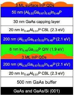
Figure 1: InP QDs co-grown on GaAs and GaAs/Si.
The researchers used solid-source molecular beam epitaxy (MBE) to produce their QD samples (Figure 1). The substrate was supplied by Germany-based NaAsPIII-V GmbH, on which the Urbana-Champaign researchers grew GaAs. The commercial substrate consisted of GaP/Si with a 4.3μm GaAsyP1-y step-graded buffer, resulting in a relaxed GaAs cap layer at room temperature. The GaAs/Si material was cleaved into smaller pieces for the QD growth.
The GaAs/Si was loaded into the MBE equipment alongside comparison pure GaAs pieces. The dot layer was produced at 480°C with a V/III ratio range of 10-30. A surface dot layer was also grown to provide easy access for atomic force microscopy (AFM).
The intervening compounds used for the AlGaInP barrier, InGaP carrier-blocking layer (CBL), and InGaP quantum well (QW) layers were designed to be lattice matched to GaAs, as determined by high-resolution x-ray and PL analysis. The barriers and CBLs prevented carriers from reaching the surface, where non-radiative recombination can take place, sapping the PL intensity. The QDs were found to have ~3.7% compressive strain. This strain is the residue of the mismatch that drives the Stranski-Krastanov self-assembly into dots.
The QD samples were prepared for PL analysis by removal of the surface InP QDs and 50nm AlGaInP before rapid thermal annealing (RTA) at 700-1000°C for between 1 second to 5 minutes. Just before PL, the 30nm GaAs capping layer, protecting the underlying aluminium (Al)-containing layers from oxidation, was also removed. The best RTA conditions for InP QD PL intensity were found to be 750°C for 5 minutes. Some InGaP QWs grown without QDs were found to perform best when subjected to 1000°C for 1 second. RTA drives out point defects from the structure, increasing PL intensity.
The PL emission (Figure 2) from the InP QDs was found to be 0.4eV blue-shifted relative to bulk InP. The higher energy bandgap is a result of the carrier quantum confinement and compressive strain in the dots. InGaP QW structures suffered a 9x degradation in PL intensity when grown on GaAs/Si, compared with pure GaAs substrates. By contrast, the InP QDs suffered relatively little impact from growth on GaAs/Si. “Strong non-radiative recombination at threading dislocations” was blamed for the reduction in InGaP QWs.
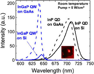
Figure 2: Room-temperature PL spectra of InGaP QW (blue) and InP QDs (black) grown on GaAs (dashed) and GaAs/Si (solid). Inset: visible emission observed from InP QDs grown on GaAs/Si.
The researchers comment: “The integrated emission intensity of InP QDs on silicon was 8x higher than that of InGaP QWs on silicon, demonstrating the viability of dislocation-tolerant, visible, phosphide-based light emitters on silicon.” They add: “A reduced diffusion length of carriers due to lateral carrier confinement also makes InP QD active regions insensitive to dislocations compared to InGaP QW structures, where carriers freely diffuse to dislocations. Finally, differences in the energy level and capture cross section for dislocation-related traps in InP and InGaP could also partially account for the observed discrepancies in dislocation tolerance.”
The PL emission spectra showed ground-state emissions of 649nm wavelength (1.91eV) and 713nm (1.74eV) for InGaP QWs and InP QDs on GaAs, respectively. The corresponding full-widths at half-maximum (FWHMs) were 24meV and 65meV. The InGaAs QW spectra also showed a shoulder around 621nm from the first excited state. The shoulder on the InP QD spectrum was attributed to a bimodal QD size distribution. The researchers comment: “The comparatively higher FWHM of InP QDs can be attributed to inhomogeneous broadening due to the distribution in QD size.”
The PL from samples on GaAs/Si were slightly red-shifted relative to pure GaAs, an effect attributed to tensile strain arising from thermal expansion mismatch between the GaAs and silicon.
Transmission electron microscope (TEM) analysis showed “misfit dislocations around the active region, an issue commonly observed with InAs DWELLs grown on silicon,” according to the team. The dot density was estimated at ~1011/cm2. In the mean, the height and diameter of individual dots were 2.4nm and 20nm, respectively, similar to InAs dots capped with InGaAs.
AFM showed the dot density to be 1.3x10¹¹/cm2, consistent with the TEM results. The density was higher than previous reports, due to “nucleation on an Al-rich surface at a relatively low growth temperature”, the researchers say. InP QDs are often grown using metal-organic vapor phase epitaxy at ~650°C. The surface QDs were around 2-3x higher than the capped dots, due to the absence of mass-transport effects into the cap layer. The surface QDs showed bimodal grouping around heights of 4nm and 7nm.
The high dot density is seen as being “essential for efficient luminescence and defect-tolerance of visible QD-based emitters on silicon”. The typical InAs QD density is around 5x10¹⁰/cm2. Cathodoluminescence suggested a threading dislocation density of 3.3x10⁷/cm2, around four orders of magnitude lower than the InP dot density.
https://doi.org/10.1063/5.0030102
The author Mike Cooke is a freelance technology journalist who has worked in the semiconductor and advanced technology sectors since 1997.


