


News: Photovoltaics
5 November 2020
III-V photovoltaics for IoT dust
IBM T J Watson Research Center in the USA has developed a wafer-level package process to integrate III-V photovoltaic (PV) devices with electronic components with a view to Internet of Things (IoT) applications [Ning Li et al, Adv. Mater. p2004573, published online 23 October 2020]. The researchers claim that their dust-sized devices “achieve higher power density than all prior micro-PVs on silicon (Si) and silicon-on-insulator (SOI) substrates”.
The team sees their work as contributing to realizing distributed ‘edge’ computing where the processing and storage of data is performed close to where it is used, reducing response times and increasing bandwidth. Power for such systems needs to be autonomous.
IoT dust systems could see deployment in authentication, industrial monitoring, block chain payment/transaction encryption, healthcare, sensing and tracking, and defense. Presently, such devices need power supplies of more than 100μW, up to ~100mWs for high-data-rate artificial intelligence (AI) and neuromorphic computing.
The researchers report: “We show that our monolithically integrated micro-PV is the first demonstration of high-throughput and low-cost manufacturing of small edge computers.” III-V semiconductor heterostructures were used to achieve high power density. The high-throughput and low cost is key to deployment – previous wirebond and chip-stacking attempts have suffered throughput and cost limitations.
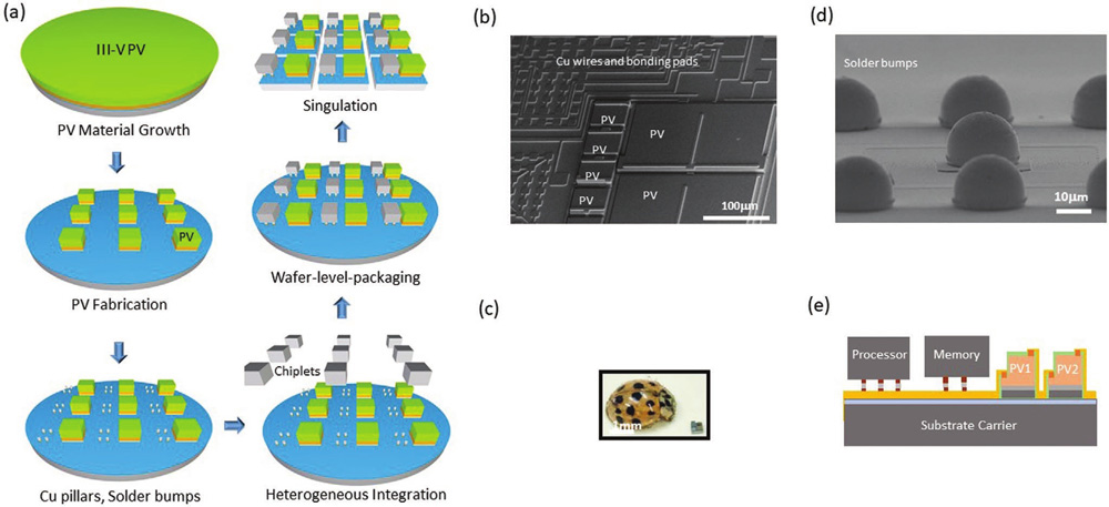
Figure 1: (a) Schematic package flow: III–V PV growth on SOI substrate, PV mesa etched down to buried oxide (BOX), PV cell fabrication and copper (Cu) interconnect, Cu pillar and solder bump formation for chip packaging, wafer-level selective bonding of fabricated chips, and chip singulation using deep Si reactive ion etching (RIE). (b) Scanning electron microscopy image of wiring and pads for pillar and solder bumps. (c) Picture of dust device with ladybug to illustrate relative size. (d) Scanning electron microscopy image of solder bumps. (e) Cross-section schematic of small computer system.
The PV components were fabricated on SOI substrates (Figure 1). The interconnection to the processor and memory components was through electroplated copper with copper pillars attached on solder bumps. Separately fabricated processor and memory ‘chiplets’ were attached in a wafer-level process. Singulation used deep reactive-ion etch to give low kerf loss.
The researchers envisage the devices being run using energy transfer via laser or high-power LED illumination. The energy could then be stored in on-chip batteries or used directly. Two types of PV cell were fabricated: large ones designed to deliver a photocurrent at around a 1V level, while the smaller ones increased the voltage for particular needs. The PV cell sizes ranged from 45μmx45μm to 400μmx200μm.
The researchers see some advantages arising from the use of LEDs rather than laser diode sources: the larger spot size gives higher tolerance to misalignment, and LEDs are less likely to damage eyesight. IBM used a two-lens collimation and focusing setup to illuminate the PV devices with high-power LEDs. The team comments: “For the case of a production line or shipping center, where automated alignment tools may be available, the alignment of the PVs and LEDs is much easier. The high-power LEDs and lens are not part of the small computer. They are part of a device to power and interrogate the small computer.”
The PV structures also enabled communication at rates up to 1Mbit/second with simultaneous data and power transmission from LED sources. The resistance-capacitance (RC)-limited 3dB frequency bandwidth (f3dB) for 20μmx20μm devices was calculated at 7.5GHz. The researchers report: “The RC-limited f3dB is much higher than the previously reported PV as data receiver due to small size and thus small capacitance.” A thicker absorber layer of ~2.3μm reduces the bandwidth to 1.5GHz due to the longer diffusion time through the base/absorber region. Silicon PV cells have much lower bandwidths (~100x).
Illumination from laser diodes and LEDs is generally narrower in wavelength spread than that emanating from the sun. This enables the use of tuned PV devices with higher power-conversion efficiencies for near-band-edge illumination.
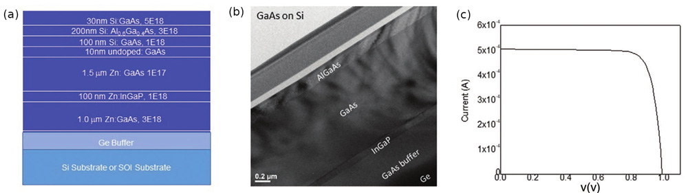
Figure 2: (a) Schematic layer stack of GaAs PV device on 6°-offcut Si substrate. (b) Cross-sectional transmission electron microscope image of GaAs PV device. (c) Current-voltage characteristics of GaAs-on-Si PV with 1mW 830nm light input.
The researchers used a 1.5μm gallium arsenide (GaAs) absorber structure (Figure 2), which can achieve power-conversion efficiencies of ~60% with 800nm 10W/cm2 light input, compared with just 25% for 1.5μm Si-based devices with 450nm illumination. Increasing silicon thicknesses to 9μm enables a higher efficiency of 35% with 650nm light.
A 100μmx100μm GaAs-based PV device with anti-reflective coating achieved 40% power conversion under 830nm 1mW illumination. This is close to what can be achieved with structures grown on GaAs substrates (45%), which in turn are approaching the theoretical limits.
The III-V-materials were grown using a two-step process with cyclic annealing to reduce heteroepitaxial defect densities. While the 1.5μm absorber was relatively thin, the overlying window layers were thicker than usual in solar PVs to reduce sheet resistance. The researchers report that they have also produced PV structures on silicon with wider-bandgap absorber materials such as aluminium gallium arsenide (AlGaAs) and indium gallium phosphide (InGaP) with a view to higher output voltage needs.
The penalty in open-circuit voltage for the 100μmx100μm GaAs PV on Si, compared with on GaAs, was around 19% at low illumination, but this reduced to around 13% at high powers of 10W/cm2.
III-V photovoltaics Photovoltaics GaAs PV SOI substrates LEDs
https://doi.org/10.1002/adma.202004573
The author Mike Cooke is a freelance technology journalist who has worked in the semiconductor and advanced technology sectors since 1997.


