


News: Microelectronics
26 November 2020
Improving p-GaN gate HEMT reliability
Hong Kong University of Science and Technology has used a gallium oxynitride (GaON) surface reinforcement layer (SRL) to boost the gate voltage window and long-term reliability of p-type gate GaN-channel power high-electron-mobility transistors (HEMTs) [Li Zhang et al, IEEE Electron Device Letters, published online 10 November 2020]. The team claims “the highest maximum gate voltage for a 10-year lifetime”, compared with other reports of p-GaN HEMTs.
Team leader Kevin J Chen explains: “This main idea of this work is to reinforce the vulnerable (to hot-electron bombardment) surface region of the p-GaN layer with a stronger material, i.e. GaON. It is like replacing a glass wall with a concrete wall.”
The SRL was put at the interface between Schottky metal and p-GaN in the gate stack (Figure 1). A p-GaN gate is used to achieve enhancement-mode behavior with the device off at 0V gate potential, i.e. ‘normally off’. This is desired in power applications for reduced power consumption/waste and for fail-safe operation. The p-GaN gate structure has been commercialized due to its “good balance among performance, reliability, and manufacturability,” the researchers explain.
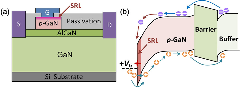
Figure 1: (a) Schematic cross section of p-GaN gate HEMT with SRL and (b) energy-band diagram for gate region at forward gate bias.
Although a Schottky contact with the p-GaN enables a lower gate leakage than for devices with an ohmic contact, the gate potential is then limited to less than 7V, due to time-dependent gate breakdown (TDGB) behavior. At the same time, the optimum gate potential for low dynamic on-resistance is in the range 5-6V, giving a very small operation window. Parasitic inductance can lead to oscillation/ringing effects that threaten the performance of the device by allowing the gate potential to wander outside the safe window.
The TDGB has been blamed on a small number of ‘hot’ electrons from the two-dimensional electron gas (2DEG) channel spilling over the aluminium gallium nitride (AlGaN) barrier layer into the p-GaN depletion region. These electrons are then accelerated in the electric field under the gate, reaching their highest kinetic energy at the metal/p-GaN interface region.
The researchers comment on the effect of the SRL: “With a wurtzite crystalline structure and a wider bandgap of ~4.1 eV, GaON tends to exhibit enhanced covalent bond strength and is expected to present stronger immunity to the bombardment of hot electrons generated under forward gate bias. Thus, GaON plays the role of reinforcing the GaN surface layer against the possible covalent bond breakage induced by hot electrons.”
Chen’s team has previously reported the use of GaON in metal-insulator-semiconductor field-effect transistors (MIS-FETs).
For the p-GaN gate HEMTs, the researchers used 6-inch GaN on silicon (GaN/Si) wafers designed for E-mode p-GaN gate power HEMTs. The layer structure was 4.2μm high-resistivity GaN buffer, 420nm GaN channel, 15nm Al0.2Ga0.8N, and 100nm p-GaN cap. The cap layer was doped with ~3x10¹⁹/cm3 magnesium.
The GaON SRL was created using an inductively coupled oxygen plasma treatment, followed by 30-minute annealing at 800°C in nitrogen. The high temperature is “crucial to reconstruct the plasma-oxidized GaN surface and form a crystalline oxidation layer,” the team reports. Secondary-ion mass spectrometry (SIMS) showed oxygen penetration into the p-GaN of around 5nm.
The surface roughness was only slightly increased by the plasma/annealing needed for the SRL: 0.44nm, compared with the initial 0.42nm root-mean-square, according to atomic force microscopy.
The p-gate with SRL cap was then formed by boron trichloride (BCl3) inductively couple plasma etch. Passivation was formed by plasma-enhanced atomic layer deposition (PEALD) of 4nm AlN, and plasma-enhanced chemical vapor deposition (PECVD) of 60nm SiNx. Source/drain contact windows were then opened up for deposition of annealed titanium/aluminium/nickel/gold ohmic contacts.
The device isolation was achieved using multi-energy fluorine ion implantation. The nickel/gold gate contact was made after another contact window opening process. The devices were completed with contact pads and interconnection to the HEMT contacts.
The HEMT dimensions were 4μm gate length with 2μm contact window, along with 15μm and 2μm gate-drain/source spacings, respectively.
The threshold voltage (VTH) for the device was +1.4V for 0.01mA/mm drain current, the same as for a comparison device without the SRL. Both transistors also exhibited a low 90mV/decade subthreshold swing and a high on/off current ratio of more than 108. The 11Ω-mm specific on-resistance (RON) is described as ‘low’.
In off-state measurements, with the gate and substrate grounded to the source voltage level, the drain bias reached 740V before breakdown for 1μA/mm current. The main leakage source beyond 550V drain bias was from the substrate.
The team comments: “These results show that the deployment of SRL neither significantly modify the forward conducting characteristics (e.g. VTH and RON) nor compromise the reverse blocking capabilities of the devices.”
The forward gate breakdown voltage was increased to 12.7V from 10.5V by the SRL insertion, while reducing the gate leakage by two orders of magnitude. The team explains this as being due to “reduced effective acceptor doping concentration and higher Schottky barrier height (φb) between the gate metal/GaON interface”.
Using a Fowler-Nordheim tunneling fit to the gate current-voltage behavior, the researchers estimate φb to be 1.1eV with SRL and 0.6eV without. The higher barrier reflects the wider ~4.1eV bandgap of GaON, relative to the 3.4eV for GaN.
The breakdown voltages increased somewhat at 150°C, to 13.4V with SRL and 11.4V without, an effect tentatively attributed to “alleviation of hot-electron bombardment as a result of mitigated electron acceleration process at elevated temperature”. The two orders of magnitude reduction in gate leakage was maintained at the higher temperature.
Time-dependent gate breakdown tests were carried out at a range of biases. The failure was defined as the “critical point where gate current increases suddenly”. The SRL enabled an increased estimate of the maximum gate voltage (VG-max) for a 10-year/1% failure level of 7.8V, compared with 5.9V without SRL. The expanded gate voltage range for the SRL device is seen as providing “appreciable design flexibility for gate driver circuits”.
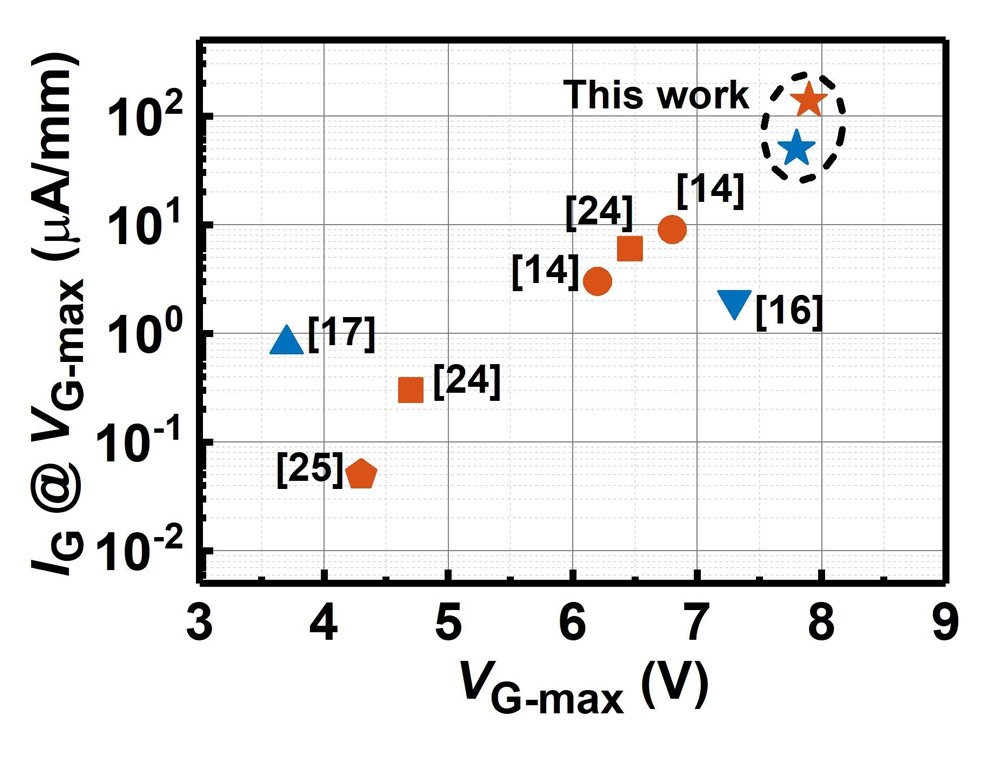
Figure 2: Comparison of p-GaN gate HEMTs with SRL (‘this work’) and other p-GaN gate HEMTs. Blue labels extracted at 25°C, orange ones at 150°C.
The researchers compared their SRL devices with reports in the literature, showing that their device gives the highest maximum gate voltage for a 10-year lifetime (Figure 2). The higher gate leakage at the higher gate stress, according to the team, “provides further evidence that the p-GaN surface region has been reinforced to better sustain the bombardment of highly energetic carriers by the deployment of GaON SRL.”
GaON GaN GaN gate HEMT HEMT SRL PECVD
https://doi.org/10.1109/LED.2020.3037186
The author Mike Cooke is a freelance technology journalist who has worked in the semiconductor and advanced technology sectors since 1997.


