


News: Optoelectronics
28 May 2020
Continuous-wave lasing from InGaN microdisk laser diodes on silicon
Researchers based in China claim the first room-temperature continuous-wave electrically pumped indium gallium nitride (InGaN) microdisk laser diode (LD) grown on silicon (Si) substrate [Jin Wang et al, Optics Express, vol. 28, p12201, 2020].
The team from University of Science and Technology Beijing, Suzhou Institute of Nano-Tech and Nano-Bionics, University of Science and Technology of China, and Tsinghua University, hope that their work could benefit optical storage, and chemical and biological sensing applications, among others. The team further suggests that such laser diodes could be used to power optoelectronic integration with III-N waveguides and visible light communication (VLC) on a low-cost mass-production silicon platform.
The smaller sizes of microdisk laser diodes, compared with conventional ridge-waveguide Fabry-Perot structures, tend to favor low threshold currents and also give higher-quality factors.
Up to now, only pulsed operation has been achieved in InGaN microdisk laser diodes. In 2018, China-based researchers from Suzhou Institute of Nano-Tech and Nano-Bionics, University of Science and Technology of China, and Changchun Institute of Optics Fine Mechanics and Physics reported pulsed operation of microdisk structures on silicon [www.semiconductor-today.com/news_items/2018/mar/sin_120318.shtml].
The latest research began their work by optimizing the p-type gallium nitride/aluminium gallium nitride (GaN/AlGaN) superlattice cladding layers to reduce series resistance and optical losses. In particular, the carbon contents of the layers were reduced from 2x10¹⁸/cm3 to 2x10¹⁷/cm3 by slowing the growth rate from 17.4nm/minute to 8.7nm/minute, respectively.
The growth rate was slowed down by reducing the flow rates of the Ga and Al metal-organic precursors. Another technique to reduce carbon content would have been to increase the deposition temperature, but this would damage the InGaN active light-emitting layers. The slower growth enabled a lower growth temperature, avoiding InGaN damage.
Top-ring contact 20μm-radius (10μm inner ring) micro-LDs with reduced-carbon p-cladding showed reduced series resistance and optical loss. In particular, the threshold current was reduced from 240mA to 60mA.
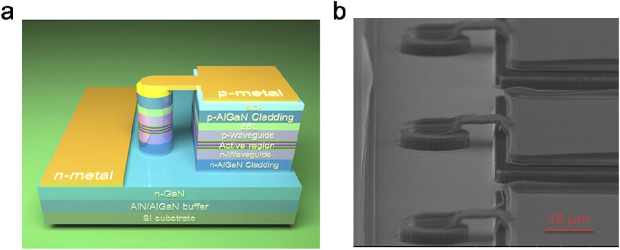
Figure 1: (a) Schematic of GaN-based microdisk laser on silicon with air-bridge electrode structure, (b) bird’s-eye-view scanning electron microscope image of microdisk laser diode array.
Unfortunately, the thermal management properties of the 20μm laser diode were not sufficient to achieve room-temperature continuous wave (CW) operation. By contrast, when the reduced-carbon p-clad material was fabricated into 8μm-radius microdisk laser diodes (Figure 1), using previously reported techniques, a CW lasing threshold current was achieved around 18mA (Figure 2). Under pulsed operation, a slightly lower threshold of 15mA was found.
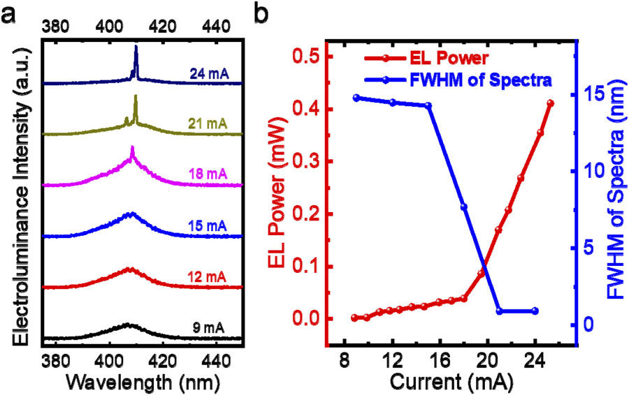
Figure 2: (a) Electroluminescence spectra of microdisk laser diode under CW current injection. (b) Full-width at half maxima of spectra and light output power as function of CW injection current.
The researchers see the relatively small difference in threshold as “indicating that the influence of self-heating on the device performance was greatly suppressed because of the improved epitaxial structure and reduced microdisk size”.
The emission peak was around 407nm wavelength, and the full-width at half maximum (FWHM) linewidth reduced to around 0.5nm above threshold injection.
InGaN microdisk laser diode InGaN Silicon substrate
https://doi.org/10.1364/OE.391851
The author Mike Cooke is a freelance technology journalist who has worked in the semiconductor and advanced technology sectors since 1997.


