


News: Optoelectronics
7 May 2020
Green vertical-cavity surface-emitting laser enabled by curved mirror process
Japan’s Sony Corp has extended its curved-mirror vertical-cavity surface-emitting laser (VCSEL) process to ~515-518nm green wavelengths [Tatsushi Hamaguchi et al, Appl. Phys. Express, vol13, p041002, 2020]. In previous work, Sony produced low-threshold 445nm blue VCSELs with curved-mirror back reflectors [www.semiconductor-today.com/news_items/2019/apr/sony_030419.shtml].
The curved mirror allows longer cavity lengths through the reduction of diffraction effects. The longer lengths are desired to take advantage of the higher thermal conductivity of GaN relative to distributed Bragg reflectors (DBRs) for heat management.
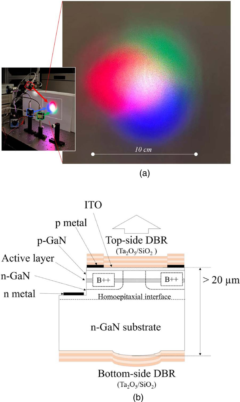
Figure 1: (a) Picture of screen irradiated by three VCSEL outputs, red, blue and green. Inset: measurement set up. (b) Schematics of green VCSELs with curved bottom mirror.
The researchers combined their device with existing blue and red VCSELs to produce white light, claimed as a first such demonstration (Figure 1). The team comments: “This is the first example of a VCSEL-based full-color light source, which will have a great impact on the industry.”
The Sony researchers point out that smartphones, tablets, laptops, smartwatches and other devices with displays emit light over a wide range of wavelength, only a small fraction of which is visible, wasting much of the input power. They suggest that highly directive, low-power VCSELs would be able to deliver sufficient power with lower losses in applications such as retinal scanning displays.
The team also hopes that its curved-mirror technique could be applied to III-arsenide and III-phosphide VCSELs, enabling emission wavelengths from ultraviolet, through visible, and down to the infrared regions of the electromagnetic spectrum.
The epitaxial material for the green VCSEL consisted of metal-organic chemical vapor deposition (MOCVD) III-N layers on (20−21) n-GaN substrate. The active region consisted of four indium gallium nitride (InGaN) quantum wells separated by GaN barrier layers. The use of the (20-21) crystal orientation avoids unwanted piezoelectric fields inhibiting low laser threshold currents due to strain in the high-indium-content InGaN layers needed for green emissions.
The p-side fabrication created a 30nm indium tin oxide (ITO) transparent conductor contact and a 11.5-pair tantalum oxide (Ta2O5)/silicon dioxide (SiO2) distributed Bragg reflector with a designed reflectivity peak wavelength of 515nm. The n-contact was made through a hole etched into the top-side layers to the n-GaN substrate. The metal contacts for both the ITO and n-GaN were titanium/platinum/gold. A 4μm-diameter circular current aperture was defined by a boron (B) implant.
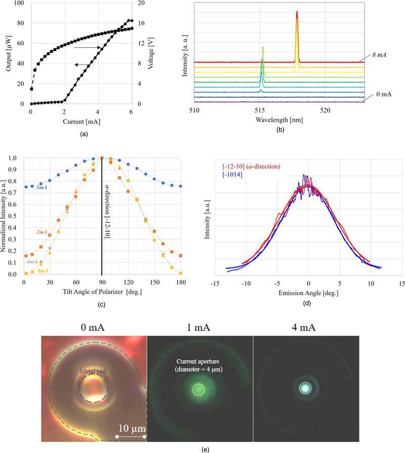
Figure 2: (a) Current–voltage and current–light output power (I–V and I–L) curves. (b) Emission spectra for 0–8mA. (c) Polarization angle measured across threshold current. (d) Far-field pattern (FFP) at 6mA. (e) Near-field image below and above threshold.
The bottom curved mirror was fabricated by thinning the wafer to 20μm, applying a 26μm-diameter resin disks, heating to 200° to convert the disks to droplets, and performing reactive-ion etch. The resin droplets acted as a sacrificial mask for the etch, resulting in a lens-shaped curved surface. The bottom mirror was completed with 14 pairs of Ta2O5/SiO2.
The VCSEL was finally diced and mounted p-side up in a 5.6mm TO-CAN package without a submount. Testing was in continuous wave mode with the VCSEL on a Peltier cooler at 25°C. The laser threshold current was 1.8mA, corresponding to 14.4kA/cm2, with a wall-plug efficiency less than 0.1%.
The initial emission peak was at 515.2nm, which hopped to 517.9nm when the current was in the 5-6mA range. The 2.7nm hop suggested an effective cavity length of 18.6μm. The output light became more polarized as the injected current increased: 0.14 at 1mA, and 0.93 at 8mA. The polarization angle was fixed relative to the III-nitride crystal structure and was in the a-direction ([-12-10]). The far-field emission pattern was approximately Gaussian with a full-width at half maximum (FWHM) divergence of around 9°.
VCSEL GaN InGaN GaN Substrate MOCVD
https://doi.org/10.35848/1882-0786/ab7bc8
The author Mike Cooke is a freelance technology journalist who has worked in the semiconductor and advanced technology sectors since 1997.


