


News: LEDs
26 March 2020
Micro-scaling of indium gallium nitride blue and green light-emitting diodes
University of California Santa Barbara (UCSB) in the USA and Seoul Viosys in South Korea have been exploring the effects of scaling down the diameters of green and blue indium gallium nitride (InGaN) micro light-emitting diodes (LEDs) [Jordan M. Smith et al, Appl. Phys. Lett., vol116, p071102, 2020]. Often external quantum efficiency (EQE) in LEDs is reduced as dimensions scale down due to non-radiative recombination at device surfaces.
The UCSB/Viosys team found a marked such effect for the blue devices, but the green LEDs were less affected. Indeed, at LED diameters less than 10μm, the green devices became more efficient than the blue ones.
The researchers also suggest that there may be a similar diameter crossover effect for red InGaN LEDs in comparison with the standard commercial aluminium gallium indium phosphide (AlGaInP) products. One would expect red InGaN LEDs to suffer even higher carrier localization effects, further reducing the surface recombination velocity (SRV).
The team reports: “The SRV in red AlGaInP is even higher than that in blue InGaN, while the SRV of red InGaN is lower than that of green InGaN. Thus, it is likely that a similar crossover in EQE... exists between red AlGaInP and red InGaN micro-LEDs, where InGaN devices would win out at smaller sizes.”
The researchers hope that factors such as increased brightness and reliability, reduced power consumption, longer life-times and smaller form factors for InGaN micro-LEDs will lead to display applications in 4K TVs, smartphones and augmented-reality (AR) glasses.
The team reports: “There are no previous reports of micro-LED EQE trends for mesa dimensions below 5μm, despite commercial demands.”
The researchers have developed a combine dry etch process, avoiding the need for precise separate steps (Figure 1). The dielectric aperture was formed by a self-aligned wet undercut etch. The process began with blanket depositions of 30nm indium tin oxide (ITO) transparent conductor, 300nm silicon dioxide (SiO2) and 200nm silicon nitride (SiN) on the LED epitaxial wafer.
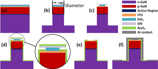
Figure 1: LED fabrication: (a) blanket ITO/SiO2/SiN deposition; (b) dry mesa etch; (c) selective SiO2 undercut; (d) passivation sputter deposition; (e) SiO2 lift-off; and (f) dry etch of passivation and formation of contact/probe pads.
Dry etch was used to define the mesa, while the SiO2 was selectively undercut using buffered hydrofluoric (HF) acid solution. Passivation was provided by sputtering 250nm aluminium oxide (Al2O3). A lift-off process selectively removed SiO2 material using vapor HF. Dry etch of the Al2O3 exposed the n-GaN contact layer. Finally, reflective 600/100/600nm aluminium/nickel/gold (Al/Ni/Au) common contact/probe-pads were applied using electron-beam evaporation and lift-off.
The fabrication was performed on commercial epitaxial material on c-plane sapphire designed for green (532nm wavelength) and blue (467nm) LEDs. The diameters of the circular LEDs ranged from 1μm to 30μm. The devices were fabricated in one run to limit the effects of run-to-run process variations. The output light was collected on the sapphire side of the devices.
The EQE of the blue LEDs declined as the diameter reduced to 5μm, but remained at about the same level in the range 1-5μm (Figure 2). By contrast, the green LEDs showed less decline in performance over the complete 1-30μm range of diameters.
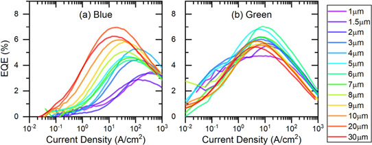
Figure 2: EQE versus logarithmic current density for 1-30μm devices for (a) blue and (b) green wavelengths. Results for devices with the highest measured peak EQE are shown.
The blue devices also showed a shift to increasing current density of the peak EQE value. Again, the green LED peak current density was apparently unaffected.
In terms of the peak EQE value, both devices had fairly constant performance in the 10-30μm diameter range, with the main decline in the blue LED performance coming over the 1-10μm section. The green devices in fact showed superior peak EQE below 10μm diameter.
The researchers comment: “This crossover is remarkable since it is well known that the internal quantum efficiency (IQE) of bulk green InGaN material is lower than that of blue.” The lower IQE comes from lower material quality due in part to the lower growth temperature needed to maintain indium content, and to the increased strain between the InGaN and surrounding GaN layers. Other factors include in-built electric fields from the different ionic natures of the chemical bonds inhibiting radiative recombination (quantum-confined Stark effect), and increased Auger-type recombination from carrier localization due to inhomogeneity of the InGaN alloy composition.
The researchers invoke the carrier localization as a possible explanation for the higher peak EQE for green LEDs at smaller diameters. Since the carriers are trapped/localized, they are less able to travel to the LEDs surfaces, avoiding one route to non-radiative recombination.
https://doi.org/10.1063/1.5144819
The author Mike Cooke is a freelance technology journalist who has worked in the semiconductor and advanced technology sectors since 1997.


