


News: Optoelectronics
12 March 2020
Aluminium gallium nitride on silicon carbide for ultraviolet diodes
University of California Santa Barbara (UCSB) in the USA has been using silicon carbide (SiC) substrates to grow aluminium gallium nitride (AlGaN) structures aimed at 278nm deep ultraviolet (UV-C, 100-280nm wavelength) light-emitting diodes (LEDs) [Burhan K. SaifAddin et al, ACS Photonics, published online 27 January 2020]. The researchers used surface roughening of thin-film flip-chip devices to boost light-extraction efficiency (LEE) by a factor of 3 over smooth-faced LEDs.
“The ability to grow AlGaN LEDs on SiC with low TDD [threading dislocation density] opens new ways to fabricate high-brightness, high-power UV LEDs with high LEE,” the team comments. The 260-280nm wavelength range enables efficient disinfection by breaking up DNA and RNA molecules of pathogens. The researchers are keen to combat antibiotic-resistant bacteria such as Clostridium difficile (C. diff.), which is indeed difficult to kill using chemical methods. By contrast, UV disinfection reduced C. diff. levels by 30%, according to University of North Carolina researchers in 2010.
Fabricating efficient UV-C LEDs has been challenging due to a number of factors. Material quality can be improved by using SiC rather than sapphire, due to a closer lattice and thermal expansion match. However, UV-C light is strongly absorbed in SiC, unlike sapphire, due to its narrower bandgap. Indeed, sapphire is often used for UV-C LEDs for this reason.
Low-pressure metal-organic chemical vapor deposition was carried out on 2-inch 6H SiC on the silicon face of a c-plane (0001) crystal orientation. The AlGaN layers began with a 3.2μm AlN buffer grown in steps at 1200°C and 1000°C (Figure 1). The Al content was reduced with an 1100nm Al0.80Ga0.20N interlayer, and then 550nm n-Al0.60Ga0.40N grown at 1175°C. The multi-quantum well (MQW) region consisted of four pairs of 2.7nm/9nm Al0.39Ga0.61N/Al0.60Ga0.40N wells/barriers. The structure also included an AlGaN electron-blocking layer (EBL).
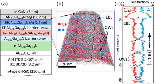
Figure 1: (a) Schematic of the UV−C LED structure. (b) APT 3D reconstruction of active layer showing EBL layer and four MQWs; (c) 1D concentration profile extracted from APT reconstruction along [0001] direction. Sampling volume dimension 20nmx20nmx50nm from dotted rectangle in (a).
The AlN buffer was crack-free due to a “novel substrate pretreatment” (annealing in ammonia/hydrogen at 1250°C) and a multi-step 3x(3D/2D) growth process reported by UCSB in 2018. The AlN buffer also achieved a reduced threading dislocation density of ~109/cm2.
The researchers used atomic probe tomography (APT) to study the material, in what the team claims was its first use on UV-LED structures.
The material was then fabricated into thin-film flip-chip devices in TO-39 headers. The SiC growth substrate was removed using a sulfur hexafluoride plasma etch. The team used potassium hydroxide solution to roughen the flipped AlN light-emission surface, increasing light output by reducing reflection back into the LED material. Also, the p-GaN thickness was reduced as much as possible, since the material is absorbing of UV-C radiation. These two measures, along with increasing the reflectivity of the p-contact, are estimated to increase the light-extraction efficiency by a factor of 3 over smooth-surface devices.
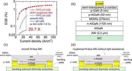
Figure 2: (a) EQE as function of current density for different 278nm UV LEDs processed from same epitaxial sample. (b) Unflipped UV LED on SiC schematic with p-side up. (c,d) Thin-film flip-chip (TFFC) UV LED (area ~0.1mm2), (c) before and (d) after surface roughening.
At 95mA injection current, the roughened UV-C LED had 7.6mW (82mW/mm2) light output power and 1.8% external quantum efficiency. The slope efficiency was 89μW/mA. The turn-on voltage was 4.3V. The LEE was estimated at 33%, the highest reported for AlGaN LEDs, the team claims.
AlGaN SiC Ultraviolet diodes UV-C LEDs SiC substrate
https://dx.doi.org/10.1021/acsphotonics.9b00600
The author Mike Cooke is a freelance technology journalist who has worked in the semiconductor and advanced technology sectors since 1997.


