


News: Optoelectronics
13 March 2020
Ranovus collaborates with IBM, TE and Senko on design and delivery of multi-vendor co-packaged optics for data centers
Ranovus Inc of Ottawa, Ontario, Canada (a provider of multi-terabit interconnect solutions for data-center and communications networks) has announced a strategic collaboration with IBM Inc, TE Connectivity and Senko Advanced Components Inc, providers of multi-terabit interconnect solutions, to create an ecosystem to design and manufacture multi-vendor solutions for co-packaged optics applications in data centers.
The collaboration leverages:
- Ranovus’ highly scalable Odin silicon photonics engine (launched earlier in March), which incorporates the firm’s multi-wavelength quantum dot laser (QDL), 100Gbps silicon photonics-based micro-ring resonator modulators and photodetectors, 100Gbps driver, 100Gbps transimpedance amplifier (TIA) and control integrated circuits in a power-efficient and cost-effective EPIC in a single chip.
- IBM’s fiber V-groove interconnect packaging technology, which is a robust and reliable assembly technique to interface optical fibers to silicon photonics devices. This process makes use of passive alignment techniques and achieves low insertion loss across a wide spectral range in both the O-band and C-band regimes. The solution is scalable in physical channel count and the automated process provides a path to high-volume manufacturing of co-packaged optics.
- TE’s co-packaged (CP) fine-pitch socket interposer technology, which enables integration of small chipset and optical engine component technologies into high-value co-package assemblies with reworkable and interoperable interfaces. The signal integrity performance of the CP fine-pitch socket interposer technology can be critical to 100Gbps high-density electrical packaging requirements. The integration of TE’s thermal bridge technology completes the assembly by providing an innovative solution for thermal management of the switch, serializer/deserializer (SerDes) and optics necessary for high reliability and long operating life.
- Senko’s fiber-optic connectivity solutions for optical coupling, on-board/mid-board and faceplate to support 100Gbps/lane-and-beyond co-packaged optics equipment designs include low-profile and precision fiber coupler assemblies, micro-sized on/mid-board connectors, reflow-compatible connector assemblies and space-saving connector options for faceplate. These will provide more efficiency, scalability and flexibility in designs for co-packaged optics equipment.
With data-center traffic growing at an unprecedented pace, the networking infrastructure needs to scale in capacity while maintaining its total power consumption and footprint, notes Ranovus. Today’s disaggregated Ethernet switch IC and optical module architecture does not provide the scalability required to support the future growth of the data centers, adds the firm. Co-packaging of optics and Ethernet switch ICs is a natural next step to reduce the power consumption burden of the electrical I/Os in the data-center networking equipment. The transition of the Ethernet switch IC Ser/Des from 50Gbps to 100Gbps, in 25.6Tbps and 51.2Tbps switch configurations, presents a unique inflection point in the architecture of the Ethernet switch systems, recons the firm.
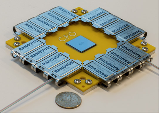
Picture: Ranovus’ Odin 32 co-packaged optics configuration for 51.2T Ethernet switch application.
“Ranovus’ Odin platform was conceived with miniaturized components such as micro-ring resonators in a monolithic electronic and photonic integrated circuit to deliver highly scalable solutions in support of single- and multi-wavelength applications,” says chief technology officer Georg Roell. “We are delighted to contribute our IP and create an ecosystem to remove a major hurdle for the adoption of co-packaged optics solutions for data centers,” he adds.
“IBM is enthusiastic to bring to this collaboration more than 45 years history in microelectronics packaging and its deep experience in optical packaging,” says Paul Fortier, senior engineer, IBM business development. “IBM’s optical assembly processes leverage our automated high-volume semiconductor packaging, and IBM’s Assembly and Test division provides the co-packaged optics ecosystem with a seamless end-to-end manufacturing capability,” he adds.
“TE is pleased to be able to bring decades of socket expertise to this co-packaging effort in the form of the fine-pitch CP socket technology,” notes TE Connectivity technologist Nathan Tracy. “In addition, TE’s thermal bridge technology is a key enabler to the high-density packaging and extreme thermal management necessary for co-packaging,” he adds.
“Senko is pleased to contribute our product designs and IP to enhance the design capability, scalability and flexibility for the co-packaged optics embedded products,” says Tiger Ninomiya, business development/product line manager at Senko. “Innovative optical connectivity solutions are key to making co-packaged optics’ solutions a success in the market.”


