


News: Optoelectronics
4 March 2020
Indium phosphide buffers on silicon for III-V laser diodes and data photonics
Bei Shi and Jonathan Klamkin of University of California Santa Barbara (UCSB) in the USA have been developing techniques to grow indium phosphide (InP) buffer layers on top of on-axis (001) silicon (Si) with a view to silicon photonics (SiPh) and, in particular, III-V laser diodes [J. Appl. Phys., vol127, p033102, 2020].
Reducing defect levels in the III-V semiconductor materials that can generate light is key to successful lasing with high efficiency. Shi and Klamkin used a range of techniques to reduce the surface defect density to 4.5x10⁷/cm2, along with producing laser diode structures aimed at the 1550nm infrared optical fiber communications range. Defects such as misfit (MD) and threading (TD) dislocations arise from lattice and thermal mismatches between the various material layers being grown.
The researchers point to “the ever-important need for on-chip light sources for high-capacity silicon photonic transceivers for hyperscale data centers and sensing applications”. Other potentials include microwave photonics, free-space laser communication, and light detection and ranging (LiDAR) based on III-V lasers, photodetectors, modulators and transistors.
Shi and Klamkin used a gallium arsenide (GaAs)-on-V-grooved Si (GoVS) template created by metal-organic chemical vapor deposition (MOCVD). The InP was grown in a three-step process: 435°C low-temperature (LT) nucleation, 45nm at 545°C medium temperature (MT), and 950nm at 600-630°C high temperature (HT).
Atomic force microscopy (AFM) and electron-channeling contrast imaging (ECCI) suggested that there was a trade-off between surface roughness and defect density, dependent on the thickness of the nucleation layer.
The researchers explain: “With a thinner LT-InP, more pinholes appear on the surface due to an inferior surface coverage following the InP nucleation although the surface roughness tends to be lower. In contrast, a better coverage together with apparent step flows can be obtained with the thicker InP nucleation, yet the surface defect density is higher, on the order of 109/cm2 , which can be attributed to the higher possibility of MDs evolving into TDs with the thicker LT-InP nucleation.”
Shi and Klamkin settled on a LT-InP thickness of 30nm as an optimum.
The effect of dislocation filtering was also studied, using strained-layer superlattices (SLSs). Four such SLSs were grown separated with 300nm HT-InP. The SLS structure consisted of 10 pairs of 13nm/19nm InGaAs/InP. Again there was a trade-off between undesirable features – at low SLS growth temperature the surface roughness of a final 500nm n-InP layer increased; high-temperature SLS growth, on the other hand, tended to generate stacking faults.
Surface roughness as low as 3.79nm root-mean-square was measured by AFM with 600°C SLS growth. Before SLS growth, the defect density was of the order 1010/cm2. By varying the InGaAs composition, surface defect densities could be reduced to 7.9x10⁷/cm2, at the cost of a rougher surface with a number of ‘hillocks’.
Shi and Klamkin also produced a laser structure using an InP/Si pseudo-substrate with 1.15x10⁸/cm2 defect density to grow seven 6.3nm In0.73Ga0.27As0.85P0.15 quantum wells separated by 8nm In0.73Ga0.27As0.52P0.48 barriers (Figure 1). Fabry-Perot ridge-waveguide laser diodes were fabricated. The wafer was thinned and cleaved into laser bars before mounting on a ceramic carrier for testing.
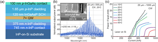
Figure 1: (a) Schematic of laser epistructure. (b) Room-temperature CW lasing spectrum at 250mA injection current – primary lasing peak at ~1593nm. Inset: 70°-tilted scanning electron microscope image of as-cleaved facet. (c) Temperature-dependent power-current curves under CW pumping.
The continuous-wave (CW) laser threshold current of 2.05kA/cm2 for a 20μmx1000μm device is described as “reasonable”. The output power reached 18mW/facet without coatings. The CW operation was possible up to 65°C. Comparison devices produced on InP substrate had a threshold of 0.675kA/cm2 and CW operation was maintained up to 95°C. Wall-plug efficiencies of 2.7% were achieved for the device on silicon, compared with 15% on InP.
Shi and Klamkin found red-shift effects at higher current injection due to self-heating. The researchers comment: “The heating originates from the reduced injection efficiency on silicon as a result of the residual threading dislocations inside the active region and the larger series resistance than lasers realized on conductive InP substrates (1.7Ω on Si and 0.8Ω on InP).”
The devices on silicon may also suffer from reduced heat dissipation arising from defects at InP/GaAs interfaces and residual stain in the InP buffer. Despite the reduced performance, Shi and Klamkin hope their work “advances the field toward the monolithic integration of InP-based on-chip light sources in the SiPh platform.”
The researchers also reduced defect densities earlier on in the growth by transitioning from the GaAs template to an In0.4Ga0.6As buffer before growing an InP buffer using the three-step process (Figure 2). The LT and HT values were 495°C and 600°C, respectively.
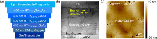
Figure 2: (a) Schematic of 1μm InP layer regrown on graded InGaAs buffer. (b) Close-up view of the InP/In0.4Ga0.6As. (c) 10μmx10μm AFM image after 1μm InP regrowth, with some pinholes identified.
A relatively thin 1.8μm InGaAs buffer was found to have a defect density of 2x10⁸/cm2, compared with just 2x10⁶/cm2 for a structure grown on pure GaAs substrates. The defect density in three-step InP buffers grown on the structure was 4x10⁸/cm2, a factor of two lower than with direct growth on GoVS. Increasing the HT to 650°C reduced the defect density to 5x10⁷/cm2 in one sample. Adding four SLS structures separated by 250nm HT-InP layers reduced the dislocation density to 4.5x10⁷/cm2 for the final 500nm InP surface layer.
Shi and Klamkin comment: “Although the surface is rougher for the InP buffer on the graded InGaAs layer, improved laser characteristics can be anticipated due to the lower defect density.”
InP Laser diodes GaAs Silicon photonics InGaAs MOCVD
https://doi.org/10.1063/1.5127030
The author Mike Cooke is a freelance technology journalist who has worked in the semiconductor and advanced technology sectors since 1997.


