


News: Microelectronics
12 June 2020
Baking and plasma-enhanced low-temperature gallium nitride atomic layer deposition
Researchers based in China and the USA have improved the crystal quality of gallium nitride (GaN) thin films on sapphire from a 350°C low-temperature plasma-enhanced atomic layer deposition process (PE-ALD) using an in-situ bake and plasma substrate pretreatment [Sanjie Liu et al, Appl. Phys. Lett., vol116, p211601, 2020].
The team – from University of Science and Technology Beijing, Hunan Normal University, Beijing National Laboratory for Condensed Matter Physics, China, and University of California Riverside, USA – hope that the process could enable improved nucleation for GaN-on-sapphire growth.
Low-temperature growth is attractive since substrates such as sapphire, or silicon, have a large thermal expansion mismatch with GaN. Standard high-temperature growth processes, typically 800-1100°C, are limited by the risk of large biaxial stress and even cracking developing in the thin-film material, degrading device efficiency and crushing production yields.
The researchers comment: “Since ALD depends dramatically on the surface reactions, the initial nucleation step influences the crystalline quality of deposited GaN.” GaN ALD on sapphire tends to result in polycrystalline films.
High-quality wide-bandgap (3.4eV) GaN semiconductor material has a wide range of present and potential future applications for short-wavelength visible and near-UV light emission, high-frequency/high-power-density electronics, and so on. High-frequency power amplification of 5G wireless communication and radar signals are a particularly hoped-for coming attraction.
The PE-ALD process used triethylgallium (TEG) and an argon/nitrogen/hydrogen gas mix in the Ga and N deposition steps. The sapphire substrates were ultrasonically cleaned with a sequence of solvents: acetone, methanol, and de-ionized water.
The next preparation step was a 4-hour bake at 500°C in argon at 0.4Torr pressure in the ALD reaction chamber. Just before the PE-ALD there was a 30-second plasma treatment with argon/nitrogen/hydrogen.
The PE-ALD process temperature was at a cooler 350°C. A reference sample was also produced using substrates without the 500°C bake and plasma treatments.
X-ray diffraction analysis showed a series of peaks that could be associated with reflections from various planes of the expected GaN crystal structure. The researchers conclude: “Accordingly, we can infer that the pretreated GaN thin film is single crystalline with a hexagonal structure.”
The full-width at half maximum (FWHM) for the (002) plane reflection rocking-curve was 666arcsec, comparable to the values obtained for higher-temperature pulsed layer deposition. The non-pretreated samples gave much broader peaks, indicating the polycrystalline nature of the resulting GaN film in that case.
The calculated c-axis lattice constant of 5.200Å was close to the 5.185Å value for unstrained GaN. The c-axis strain was therefore estimated at 0.0029. The longer c-axis constant suggests that the GaN layers were under compression.
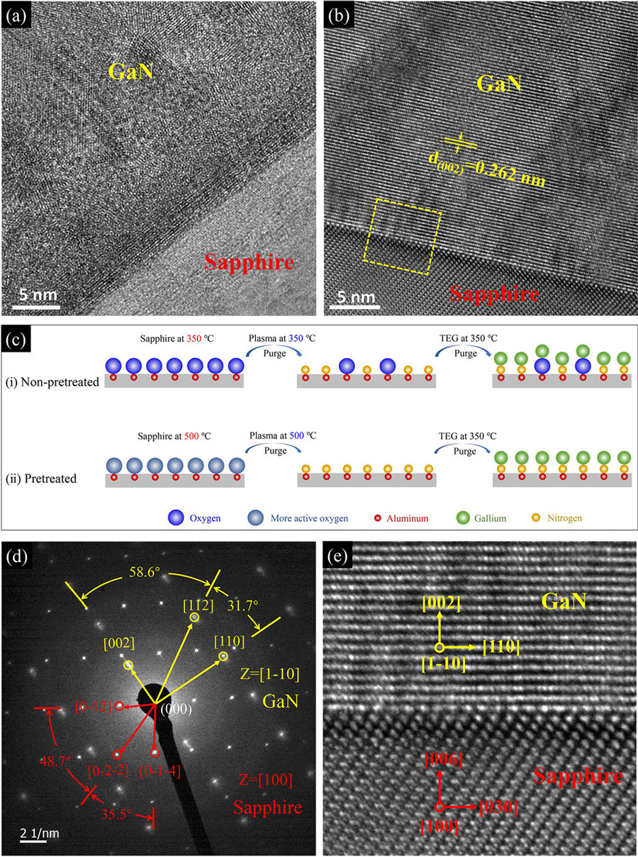
High-resolution transmission electron microscopic (HRTEM) analysis backed up the conclusions from x-ray diffraction (Figure 1). The GaN was found to be epitaxial with a [1-10]GaN//[100]sapphire plane alignment. The GaN/sapphire interface was sharp.
The researchers believe that the baking treatment activates the sapphire surface by providing energy for adatoms from the plasma treatment to diffuse rapidly over the surface to activate surface reaction sites. The plasma treatment replaces the oxygen termination of the sapphire, aluminium oxide (Al2O3), with nitrogen, enhancing subsequent GaN growth.
The team suggests the higher 500°C temperature enables such replacement to be more widespread, “perhaps even total”, across the surface, compared with a plasma pretreatment at the main process temperature of 350°C.
X-ray photoelectron spectral (XPS) depth profiling revealed carbon contamination in the range 3-7% and oxygen of 9-12% (Figure 2).
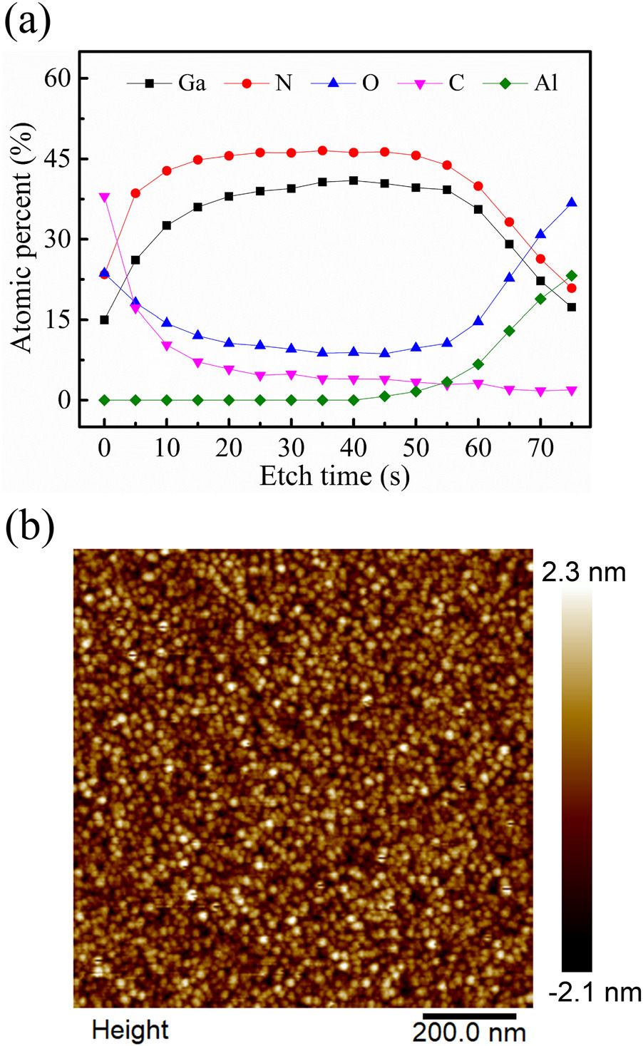
Figure 2: (a) XPS depth profile and (b) AFM image of pretreated GaN thin film.
The high level of oxygen was blamed on the use of a quartz (SiO2) tube plasma source in the ALD reaction chamber. The replacement of quartz with a stainless-steel hollow cathode for the plasma generation has been found to reduce such contamination.
The carbon came from the metal-organic TEG component. The XPS study also showed the GaN layer to be nitrogen-rich.
The surface roughness was assessed using atomic force microscopy (AFM), which gave a root-mean square value of 0.64nm for the pretreated GaN layer. Surface roughness of GaN layers produced using metal-organic chemical vapor deposition (MOCVD) on sapphire is around 2nm.
GaN GaN-on-sapphire PE-ALD MOCVD
https://doi.org/10.1063/5.0003021
The author Mike Cooke is a freelance technology journalist who has worked in the semiconductor and advanced technology sectors since 1997.


