


News: Microelectronics
19 June 2020
Boosting mobility in indium aluminium gallium nitride barrier heterostructure
Taiwan’s National Chiao Tung University has used a gallium nitride interlayer (IL) to improve the performance of indium aluminium galllium nitride (InAlGaN)-barrier high-electron-mobility transistors (HEMTs) on low-cost silicon [Min-Lu Kao et al, Appl. Phys. Express, vol13, p065501, 2020]. The team claims that their work demonstrates the first high-electron-mobility performance in InAlGaN-barrier HEMT structures.
III-nitride devices are being developed for high-frequency and high-power electronics serving the millimeter-wave part of the electromagnetic spectrum (30-300GHz, or ‘extremely high frequency’/EHF). Such radio signals are proposed for 5G wireless telecommunications and various flavors of radar.
Up to now, InAlGaN-barrier HEMTs have suffered from low mobility, compared with AlGaN- and InAlN-based devices. InAlGaN-barrier structures could result in higher polarization charge density, with potential benefits for high-power/high-frequency operation. The higher polarization level results in high sheet carrier density in the two-dimensional electron gas (2DEG) channel. Unfortunately, carrier scattering from rough interfaces between layers severely impacts mobility, increasing sheet resistance.
Experience with AlN and InAlN barrier layers suggests that a GaN IL could improve mobility in InAlGaN structures. The use of silicon should reduce material costs and enable economies of scale based on the larger substrates that are commercially available.
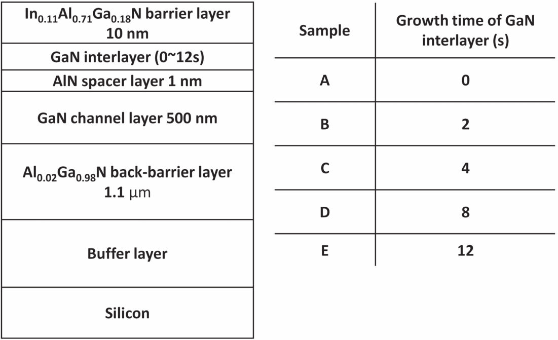
Figure 1: Schematics of InAlGaN/GaN HEMT material for samples A–E.
The researchers used 6-inch (111) silicon substrates to grow the various heterostructures (Figure 1) by metal-organic chemical vapor deposition (MOCVD). The buffer between the silicon substrate and device layers consisted of 250nm AlN nucleation and 600nm AlGaN transition layers. The InAGaN quaternary barrier was grown at 875°C temperature and 100Torr pressure. The GaN IL was grown at 1080°C at the same pressure. The thickness was varied by changing the growth time over the range 0-12s, resulting in five samples labeled A-E.
Atomic force microscopy of the samples showed reduced occurrence of spiral hillocks on the surface with the 2s GaN IL (sample B), compared with 0s (sample A, no GaN IL), or with 12s growth (sample E). The reduced hillock formation in sample B suggests that ‘step-flow’ growth is enabled, resulting in a smoother surface and reduced interface roughness deeper in the sample. The hope would be that smoother interface roughness would decrease carrier scattering, improving mobility.
The GaN has a higher vapor pressure relative to the subsequent InAlGaN barrier. The high vapor pressure is associated with decomposition of the GaN IL. It is suggested that too long growth of the IL results in a degraded surface for the InAlGaN barrier to grow on.
Of course, the main interest is whether the improved surface quality results in improved electrical performance. In Hall measurements, sample B showed the lowest sheet resistance, along with the highest mobility and carrier concentration. Sample B achieved 228.2Ω/square sheet resistance, and 1540cm2/V-s electron mobility.
HEMT fabrication used chlorine plasma etch for mesa isolation, electron-beam evaporation and annealing of titanium/aluminium/nickel/gold ohmic source-drain electrodes, nickel/gold for the gate electrode, and 100nm plasma-enhanced chemical vapor deposition (PECVD) silicon nitride passivation. The gate length was 170nm, while the source-drain spacing was 2μm. The gate was placed in the middle of the source-drain gap.
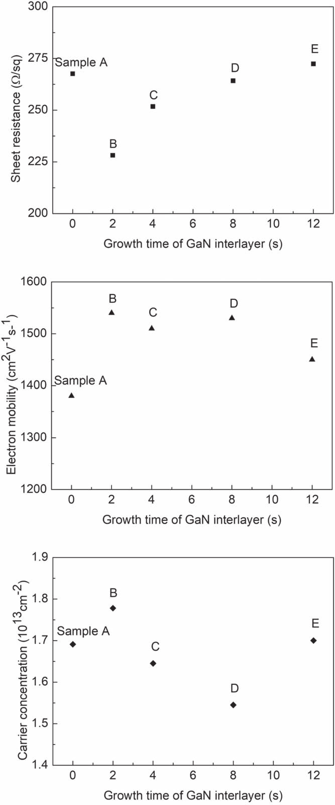
Figure 2: Sheet resistance, electron mobility, and carrier concentration as a function of sample growth time.
A HEMT based on sample A achieved a maximum drain current density of 943mA/mm, compared with sample B’s 1490mA/mm, at a 2V gate-source potential difference and 10V drain bias. The higher electron mobility of sample B also results in a higher peak extrinsic transconductance of 401mS/mm at 2V gate, compared with 204mS/mm for sample A.
The researchers offer two possible explanations for sample B’s better HEMT performance: “(1) alloy and interface roughness scattering are effectively suppressed due to the improvement of the interface roughness, thus enhancing the electron mobility for sample with GaN IL; (2) compared to the sample with InAlGaN directly grown on AlN, the crystal quality of InAlGaN barrier layer may be improved by GaN IL due to less lattice mismatch between InAlGaN and GaN.”
https://doi.org/10.35848/1882-0786/ab8b51
The author Mike Cooke is a freelance technology journalist who has worked in the semiconductor and advanced technology sectors since 1997.


