


News: Optoelectronics
24 June 2020
EU’s COSMICC project demos full-data-transfer silicon photonics module delivering 100Gb/s
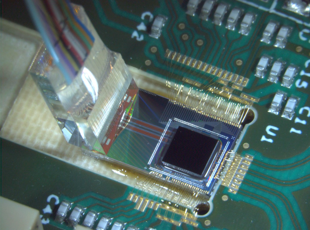
Micro/nanotechnology R&D center CEA-Leti of Grenoble, France has demonstrated a fully packaged coarse wavelength division multiplexing (CWDM) optical transceiver module with data transfer of 100Gb/s per fiber with a low-power-consumption electronic chip co-integrated on the photonic chip. The silicon-photonics-based transceiver multiplexes two wavelengths at 50Gb/s and is designed to meet the ever-increasing datacommunication demands and energy use of data centers and supercomputers.
The European Union (EU) Horizon 2020 project COSMICC (CmOs Solutions for Mid-board Integrated transceivers with breakthrough Connectivity at ultra-low Cost) further developed all the required building blocks for a transmission rate of 200Gb/s and beyond without temperature control with four 50Gb/s wavelengths and by aggregating a large number of fibers. The key breakthroughs are the development of broadband and temperature-insensitive silicon nitride (SiN) multiplexing components on silicon (Si), the integration of hybrid III-V/Si lasers on the Si/SiN chips, and a new high-count adiabatic fiber-coupling technique via SiN and polymer waveguides.
The demonstration opens the way to technology that allows a reduction in the cost, the power consumption and the packaging complexity and opens the way to reaching a very high aggregated data rate beyond terabits per second (Tb/s).
Starting with STMicroelectronics’ silicon photonics integration platform, the COSMICC project developed a CWDM silicon photonics transceiver in a packaged module at 100Gb/s per fiber. It is scalable to 400Gb/s and includes 3D assembly of a silicon photonic chip and its electronic control chip. The silicon photonic chip integrated high-performance 50Gb/s NRZ optical modulators and photodetectors, and a two-channel CWDM multiplexer and demultiplexer. The control electronics was optimized to minimize energy consumption down to 5.7pJ/bit per channel at 50Gb/s data rate.
Separately, a library of enabling building blocks for higher-data-rate data-center interconnects was built on a SiN-enhanced silicon photonics platform, including new broadband and athermal SiN components and hybrid III-V/Si lasers. SiN, which is 10 times less sensitive to temperature than silicon, will dramatically reduce the transceiver cost and power consumption by eliminating the need for temperature control and will thus contribute to a reduction in the heat output and cooling costs of mega datacenters.
CEA-Leti’s Ségolène Olivier, who coordinated the EU project, says that the development of modulators and photodetectors at 50Gb/s and their co-integration with their control electronics was a breakthrough that led to the low-power-consumption 100Gb/s transceiver module. “In addition, the new building blocks are essential for addressing the need for terabit-per-second transceivers at low cost and low energy consumption to sustain the exponential growth of data traffic in datacenters and in high-performance computing systems,” she adds. “COSMICC’s technology will answer tremendous market needs with a target cost per bit that traditional WDM transceivers cannot meet.”
In addition to CEA-Leti, COSMICC consortium members include:
- Industry: STMicroelectronics Italy & France, Vario-Optics, Seagate, Finisar.
- Academic & institutional: Université Paris Sud, Universita di Pavia, University of Southampton Optical Research Center, University of Saint Andrews, Cork Institute of Technology.
- Consultants: Ayming.


