


News: Microelectronics
23 July 2020
Transfer printing and self-aligned etching for E-mode GaN transistors
China’s Xidian University has claimed the first wafer-scale monolithic realization of normally-off, enhancement-mode (E-mode) cascode field-effect transistors (FETs) constructed from silicon (Si) and gallium nitride (GaN) components assembled through a low-cost transfer printing and self-aligned etching process [Jiaqi Zhang et al, IEEE Transactions on Electron Devices, published online 19 June 2020].
The researchers hope their technique will lead to large-scale integration and wide-spread functional-diversification of devices and circuits combining Si, GaN, and other materials. The methodology avoids expensive and complex metal-organic chemical vapor deposition (MOCVD) or wafer bonding steps.
The cascode structure (Figure 1) increases the threshold of the normally-on, depletion-mode (D-mode) GaN high-electron-mobility transistor (HEMT) by connecting it with an E-mode silicon metal-oxide-semiconductor FET (MOSFET).
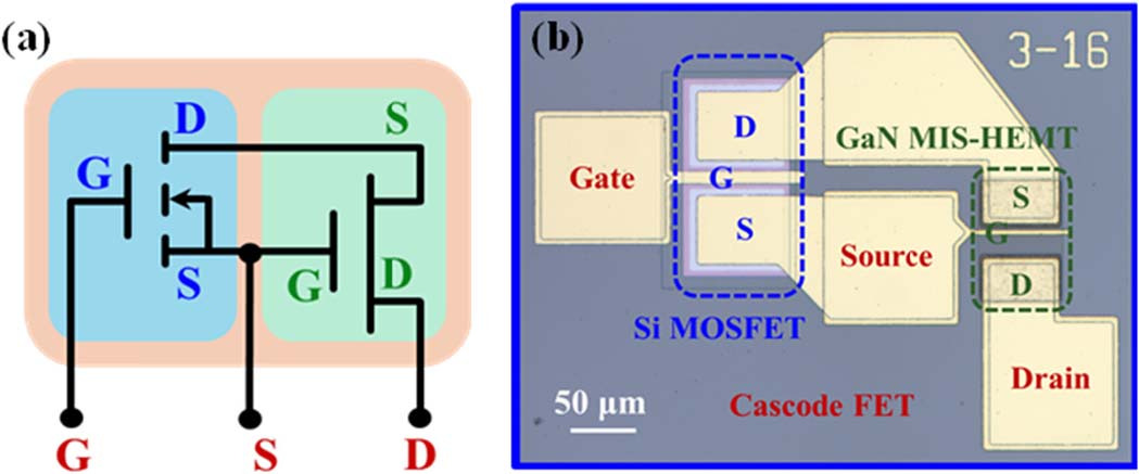
Figure 1: (a) E-mode cascode FET circuit diagram. (b) Optical photograph of fabricated device.
While GaN-based devices have great potential for high-breakdown-voltage power switching, the HEMT structure tends to result in D-mode performance, while normally-off operation is mandated for low power consumption/waste, along with fail-safe behavior.
The source materials for the cascode device (Figure 2) consisted of silicon-on-insulator (SOI) and silicon nitride/aluminium gallium nitride/GaN/sapphire (SiN/AlGaN/GaN/sapphire) wafers. The III-nitride substrate was 2-inch diameter. The 200nm-thick Si layer was boron-doped at 1x10¹⁴/cm3 concentration.
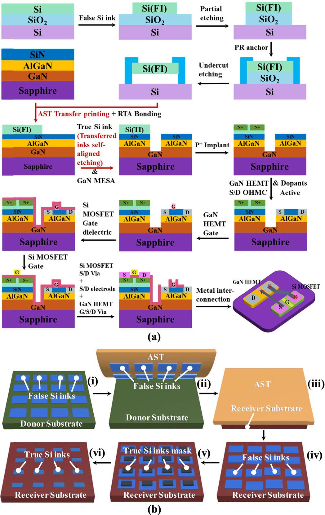
Figure 2: (a) Fabrication process flow of monolithic Si–GaN cascode FET. (b) Key steps of transfer printing and self-aligned etching technology.
The SiN cap layer electrically isolated the Si-based transistor from the underlying AlGaN/GaN material in the final cascode device. The SiN reduced leakage currents by some nine orders of magnitude.
The SOI wafer was used as donor for the Si part of the device. The silicon and silicon dioxide (SiO2) layers were etched into an array of 155μmx85μm rectangles, which the researchers refer to as ‘false inks’ (FI). The Si parts were anchored in place by photoresist, before the SiO2 was dissolved underneath, using buffered oxide etching and hydrofluoric acid.
The ‘false ink’ rectangles were transferred to the SiN/AlGaN/GaN/sapphire receiver wafer on acetone soluble tape (AST). The tape, as its name suggests, was removed by acetone, followed by ashing. The bond between the silicon and receiver wafer was strengthened by a rapid thermal anneal (RTA) at 500°C in nitrogen for five minutes.
A self-aligned reactive-ion etch (RIE) process was then performed, forming the device mesas, and reducing the bonding Si rectangles to 150μmx80μm rectangles, which the researchers then refer to as the ‘true inks’ (TI). The reduction in size takes account of the potential for the rectangles to shift around 2μm from the desired position in the AST transfer.
The Si rectangles were fabricated into MOSFETs with phosphorus implanted source/drain regions. The GaN HEMT was formed by exposing the source/drain regions and depositing and annealing titanium/aluminium/nickel/gold electrodes. The 857°C annealing process also activated the phosphorus doping.
The GaN HEMT gate consisted of nickel/gold. The Si MOSFET gate consisted of atom layer deposition (ALD) aluminium oxide and titanium/gold electrode. The source/drain contacts of the Si MOSFET were created from nickel. Nickel/gold was used for device interconnection.
The researchers have been developing AST transfer techniques for a while. This latest methodology, with a thicker AST than before, has estimated yields for the various steps: 98.25% for transfer efficiency, 93.78% for then achieving rectangles without wrinkles or cracks on the receiver substrate (‘yield’), and 96.86% for completely removing the tape (‘cleanliness’).
The transfer process enabled the researchers to reduce the interconnection distance between the E-mode Si MOSFET and D-mode GaN HEMT to the order of 100μm. Typically, chip-to-chip connections measure around 2mm. Reducing such distances are key to avoiding parasitic inductances, which introduce instability ringing effects, and increased switching losses that must be tackled in power circuits.
The researchers report: “It is estimated that the parasitic inductance can be reduced by 98.59% in monolithic integrated Si–GaN cascode FETs when compared with the conventional chip-to-chip packaged devices.”
The GaN HEMT had a gate threshold of –7.9V for a drain current of 1mA/mm at 1V drain bias. The negative threshold put the operation in the normally-on, depletion-mode category. The on/off current ratio was of the order 107. The sub-threshold swing was 96mV/decade. The gate leakage was around 10-4mA/mm. The maximum drain current was 700mA/mm with the drain bias above 8V.
The cascode circuit increased the threshold to +2.1V. The on/off current ratio continued at 107. The sub-threshold swing was somewhat negatively impacted, increasing to 141mV/decade. The gate leakage was reduced to around 10-5mA/mm. The maximum drain current was around 90mA/mm. The reduction reflected an increase in on-resistance: 31Ω-mm for the cascode FET, compared with 6.5Ω-mm for the GaN HEMT alone.
The researchers comment: “The ON-resistance or drive current of cascode FET depends on many factors, such as the interconnection distance between Si device and GaN device, the thickness of interconnection metal, the dimension of devices, and the threshold voltage of GaN HEMT. The large ON-resistance of cascode FET can be reduced by optimizing the VTH of D-mode GaN HEMT, matching the dimensions of Si–GaN devices, thickening the metal interconnects, and reducing the distance between Si–GaN devices.”
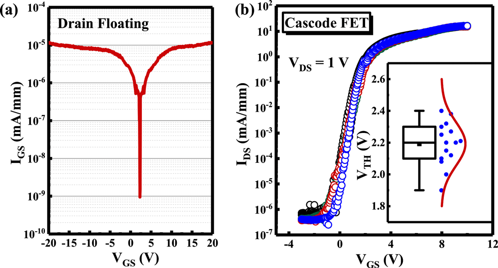
Figure 3: (a) Gate swing graph of E-mode cascode FET with drain electrode floating. (b) Transfer characteristics for series of devices.
With a gate swing between +18V and –18V, the gate leakage remained below 10-5mA/mm (Figure 3). The researchers say that this swing is greater than for competitor structures such as p-GaN gate GaN HEMTs and recess-gate GaN HEMTs. The researchers also found good uniformity of behavior over a range of separate cascode FETs.
The team found a relatively low off-state breakdown voltage of 40V, which the researchers attribute to the floating body effect of the Si MOSFET on insulating SiN structure. It is thought that the floating body Si MOSFET accumulates holes, negatively impacting the breakdown capability. This effect could be tackled by either grounding the Si MOSFET body, or implanting germanium to create a narrow-gap source region for removing the holes more effectively through recombination.
https://doi.org/10.1109/TED.2020.3001083
The author Mike Cooke is a freelance technology journalist who has worked in the semiconductor and advanced technology sectors since 1997.


