


News: LEDs
16 July 2020
Improving MOCVD tunnel junctions for gallium nitride μ-light emitting diodes
University of California Santa Barbara (UCSB) in the USA claims the lowest forward voltage for gallium nitride (GaN)-based micro-sized light-emitting diodes (μLEDs) with epitaxial tunnel junctions (TJs) grown by metal-organic chemical vapor deposition (MOCVD) [Panpan Li et al, Optics Express, vol28, p18707, 2020]. The voltage was only marginally higher than that achieved with indium-tin oxide (ITO) transparent conductive electrodes.
The UCSB team used a selective-area growth (SAG) technique to create a tunnel junction layer with perforations. The perforated holes in the TJ were used to enable escape of hydrogen during annealing aimed at activating the underlying p-GaN layer of the junction. Hydrogen passivates the magnesium acceptor levels of the p-GaN, inhibiting their ability capture electrons and create holes in the valence band. Although molecular beam epitaxy (MBE) can be used to avoid hydrogen in GaN TJ structures, MOCVD is preferred for manufacturing.
Industry is looking to use μLEDs in a range of applications: “wearable devices, large-area displays, augmented reality (AR) and virtual reality (VR), and high-speed visible light communications (VLC),” are mentioned in the paper. The potential advantages of μLEDs over liquid crystal displays (LCDs) or organic LEDs include ultra-high resolution and lower power consumption.
Hoped for benefits of using TJ structures over conventional p-electrodes include simpler fabrication, improved current spreading, and lower photon absorption. New device architectures could be enabled with direct integration of blue/green/red μLEDs in cascade structures connected with TJs.
The UCSB researchers used standard industry blue indium gallium nitride (InGaN) LED epitaxial wafers grown on patterned sapphire substrate (PSS) with a target emission wavelength around 440nm. Silicon-doped n+-/n-GaN layers were added selectively to provide the perforated tunnel junction. (Figure 1).
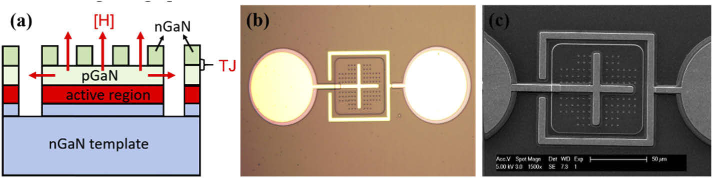
Figure 1: (a) Schematic structure of GaN TJ μLEDs through SAG; (b) microscope and (c) scanning electron microscope images of fabricated 80μmx80μm device.
In fact, the MOCVD process was preceded by growth and patterning of silicon dioxide into pillars on the p-GaN surface, which provided sacrificial structures for the hole perforations. The n+- and n-GaN layers were then grown at 1000°C with target silicon doping concentrations of 1.5x10²⁰/cm3 and 3x10¹⁸/cm3, respectively.
The LED fabrication consisted of mesa etch with silicon tetrafluoride reactive ions, removal of the silicon dioxide pillars using buffered hydrofluoric acid, 700°C annealing in nitrogen to drive out hydrogen from the p-GaN, the formation of an omni-directional reflector from 7-pairs of silicon dioxide and tantalum pentoxide layers, and the deposition of aluminium/nickel/gold for the contacts and metal pads.
Testing was carried out with diced devices mounted on silver headers and encapsulated in silicone. It was found that the emitted radiation was much more uniform across the device, compared with similar reference MOCVD TJ-μLEDs without the perforations of the n+-/n-GaN layers. In fact, the emissions were greater at the edges of the reference devices, most likely due to the sidewall out-diffusion of hydrogen during annealing.
The electrical performance of the TJ-μLEDs with perforations was also superior, giving much tighter and lower forward voltage for a given injection current density. By contrast, the reference devices showed increased forward voltage for larger areas, indicating the reduced effectiveness of sidewall out-diffusion of hydrogen during annealing in these cases.
The forward voltage for 20A/cm2 injection decreased approximately linearly with area in the reference devices: 3.7V at 100μm2 and 4.6V at 10000μm2. By contrast, the performance of similarly-sized perforated TJ-μLEDs at 20A/cm2 varied only between 3.24V and 3.31V.
The team points out that the forward voltages in the perforated TJ-μLEDs were only 0.2-0.3V higher than in conventional μLEDs with ITO electrodes on the p-GaN. The researchers comment: “To the best of our knowledge, these forward voltages are the lowest for the GaN LEDs with TJs grown by MOCVD, and comparable to the lowest for GaN LEDs with TJs grown by MBE.”
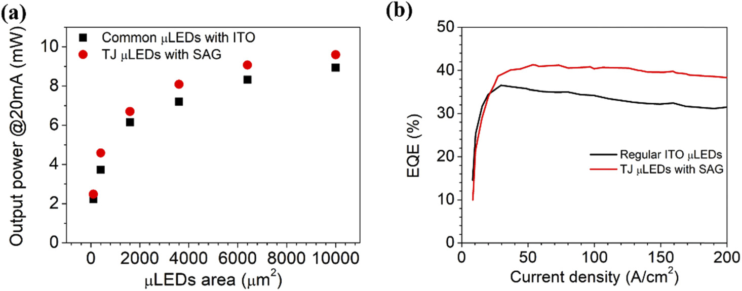
Figure 2: (a) Output power at 20mA versus various sizes in TJ μLEDs with SAG and ITO μLEDs; (b) EQE versus current density for 40μmx40μm devices.
In fact, the perforated TJ-μLEDs showed improved performance over ITO-based devices in terms of light output power at higher injection currents (Figure 2). At 20mA, the increase in output power was of the order of 10% at all device sizes.
The external quantum efficiency (EQE) was 40% at 100A/cm2 injection for a 40μmx40μm TJ-μLED, compared with 35% for a similar-sized reference device. The researchers credit the improved EQE on improved light extraction of the perforated TJ layer. Further positive factors could be “improved current spreading and reduced light absorption of the TJs”, according to the team.
GaN Epitaxial tunnel junctions MOCVD
https://doi.org/10.1364/OE.394664
The author Mike Cooke is a freelance technology journalist who has worked in the semiconductor and advanced technology sectors since 1997.


