


News: Optoelectronics
9 July 2020
Room-temperature continuous-wave 1.55μm quantum dash laser diodes on silicon
Hong Kong University of Science and Technology (HKUST) in China has claimed “the first electrically pumped room temperature (RT) CW [continuous wave] lasing results of 1.55μm quantum dash (QDash) lasers directly grown on patterned on-axis (001) Si [silicon] using metal-organic chemical vapor deposition (MOCVD)” [Ying Xue et al, Optics Express, vol28, p18172, 2020].
Previously, 1.55μm QDash laser diodes had achieved pulsed operation at RT in work by members of the HKUST team. The researchers have also recently reported on reducing threshold currents of 1.3μm-wavelength QDash pulsed laser diodes [www.semiconductor-today.com/news_items/2020/may/hkust-210520.shtml].
Such devices are desired to enable monolithic optoelectronics capabilities on silicon for communications through the optimum wavelength for 1.55μm optical fibers. MOCVD is the preferred material growth technology in III-V manufacturing, compared with much slower molecular beam epitaxy (MBE). A CW 1.55μm laser diode is the vital link to plugging the gap between silicon complementary metal-oxide-semiconductor (CMOS) electronics and photonics via silicon waveguides and outcoupling to fibers.
Direct growth of III-V laser materials is preferred over the presently successful wafer bonding techniques, which are limited in the longer term regarding scalability, cost and fabrication compatibility.
The researchers used substrates with V-groove patterns etched into the surface, enabling all epitaxial layers to be grown by MOCVD, including the initial 1.1μm gallium arsenide (GaAs) buffer. The actual laser layers were grown on a 3.1μm indium phosphide (InP) template layer.
The InP buffer included three sets of strained-layer superlattices, which each consisted of 10 periods of 12nm/34nm In0.63Ga0.37As/InP pairs. The surface roughness of the InP layer was 2nm, root mean square, according to atomic force microscopy (AFM). The threading dislocation density was estimated to be 3.6x10⁸/cm2, obtained through plan-view transmission electron microscopy (TEM).
The active region of the laser (Figure 1) consisted of three QDash-in-well structures. The InAlGaAs step contained 24% aluminium in the III-metal mix. The InGaAs cap was grown at low temperature. The structure was optimized with AFM measurements and photoluminescence (PL) experiments, which aimed at increasing emission intensity and shrinking linewidth. The final QDash density was 3.2x10¹⁰/cm2. The p-InP cladding layer was doped with zinc.
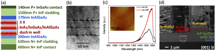
Figure 1: (a) Complete laser structure schematic; (b) TEM image of three layers of QDashes; (c) room-temperature PL of three-layer QDashes grown on Si and InP substrates (inset: AFM of QDashes); (d) tilted-scanning electron microscope view of fabricated device 6μm-wide waveguide with zoomed-in patterned V-groove silicon.
The material was fabricated into deep-etched narrow ridge-waveguide laser diodes with titanium/platinum/gold and germanium/gold/nickel/gold p- and n-electrodes, respectively. Silicon dioxide in a 550nm layer was used as passivation. Cleaved laser bars were characterized without facet coating.
Laser diodes based on traditional quantum-well structures typically use shallow-etching techniques to reduce optical losses at sidewalls (Figure 2). These considerations are not so critical for QDash emission due to reduced carrier diffusion lengths in such structures. The deep-etched structure also avoids electrical losses from current spreading in the n-contact region.
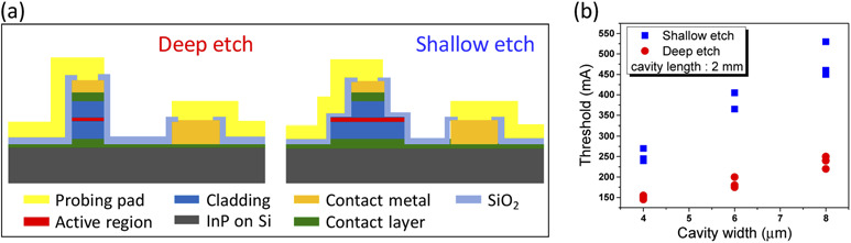
Figure 2: (a) Schematic of finalized devices with deep- and shallow-etched structures; (b) threshold currents plotted as a function of various cavity widths with 2mm cavity length.
A 6μmx1.5mm laser bar achieved a CW threshold current density of 1.3kA/cm2 and more than 44mW light output power. The device was placed on a heatsink with a temperature controller.
Spectral analysis showed the peak wavelength blue-shifted as the threshold was approached, before settling into single-mode operation at 1580nm above threshold. The laser diode emission was red-shifted relative to the PL study, due to thermally induced refraction index changes.
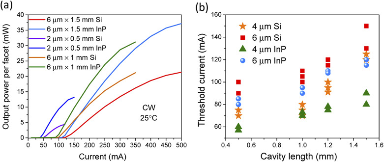
Figure 3: (a) Light output power versus current curves of lasers on Si and native InP substrate; (b) threshold current distribution of QDash lasers on silicon compared with lasers on InP at various cavity lengths and widths.
The researchers compared their devices on silicon with the same structures produced on InP substrates (Figure 3). In fact, the InP-based devices were found to have “somewhat lower” thresholds compared with QDot laser diodes reported in the scientific literature in work by University of Kassel, Germany.
In real systems, laser diodes need to operate at above room temperature due to electrically induced heating. The reduced threshold performance at increased temperature had a T0 characteristic of 44.8K between 25°C and 50°C on silicon. The T0 value reduced above that to 27.11K up to 59°C. The T0 for the device on InP was 41K between 25°C and 60°C. A higher T0 indicates a slower degradation in threshold performance.
Both silicon- and InP-based devices were able to sustain pulsed lasing performance up to 100°C. The silicon-substrate threshold current density was 555A/cm2 at room temperature with 400ns pulses at a 0.5% duty cycle. Output power reached more than 360mW. The T0 values for silicon- and InP-substrate laser diodes were around 60K in pulsed mode.
GaAs InP InGaAs Quantum dash lasers MOCVD
https://doi.org/10.1364/OE.392120
The author Mike Cooke is a freelance technology journalist who has worked in the semiconductor and advanced technology sectors since 1997.


