


News: LEDs
30 January 2020
Patterned sapphire silica substrate for ultraviolet light-emitting diodes
Researchers based in China and the USA have used a patterned combination of sapphire substrate and silica (SiO2) layer to improve the performance of ultraviolet light-emitting diodes (UVLEDs) [Hongpo Hu et al, Nano Energy, vol69, p104427, 2020]. The enhanced light output was due to a combination of improved crystal quality of the III-nitride light-emitting material and a boost in light extraction efficiency (LEE) from reducing internal reflection and absorption of the generated photons.
The team from Wuhan University, HC SemiTek Corp, University of Science and Technology of China, Huazhong University of Science and Technology in China and University of Michigan in the USA see the technology as having potential for increasing the performance of LED-based solid-state UV light sources for curing, water purification, sterilization and phototherapy.
The researchers used three types of sapphire substrate: flat (FSS), patterned (PSS) and patterned with silica array (PSSA). The pointed cones of the PSS were created using thermal reflow of patterned photoresist and inductively coupled etching. With the PSSA the pointed cones were etched into a 2μm plasma-enhanced chemical vapor deposition (PECVD) silica layer. The etch was continued down into the sapphire substrate.
The effect of the patterned sapphire was to redirect dislocations in aluminium gallium nitride (AlGaN) growth, bending their path so that they annihilate rather than threading through the indium gallium nitride (InGaN) light-emitting active layers. Such dislocations become centers for electron-hole recombination without the emission of UV photons, sapping efficiency.
The patterned sapphire technique is not as effective in AlGaN, compared with GaN-based devices. This is related to the stronger sticking of Al, compared with Ga, in the growth process. This generates misoriented crystal growth. One effect of the silica array layer is to reduce misoriented crystal regions.
The nucleation for III-N deposition consisted of 20nm sputtered AlN. Further growth was by metal-organic chemical vapor deposition (MOCVD) with trimethyl-metal and ammonia precursors. The n- and p-type doping were via silane (SiH4) and bis(cyclopentadienyl)magnesium (Cp2Mg), respectively. Hydrogen and nitrogen were used as carrier gases.
The final epitaxial structure (Figure 1) was completed with a 720°, 20 minute thermal anneal to activate the Mg doping.
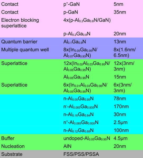
Figure 1: UVLED epitaxial structure.
The material was fabricated into LEDs with a 1.25μm mesa etch to expose the n-AlGaN contact layer. The p-GaN contact layer was covered with an annealed indium tin oxide (ITO) transparent conductor current-spreading layer. Chromium/platinum/gold were evaporated to create both the n- and p-electrodes of the diode structure. The wafer was thinned to 120μm by grinding and polishing. The 254μmx685μm chips were then singulated.
The threading dislocation density (TDD) was assessed using x-ray diffraction (XRD) and scanning transmission electron microscopy (STEM). The TDD in III-N material grown on flat sapphire is typically of the order of 1010/cm2. The estimate from the STEM analysis gave values for the PSS and PSSA samples of 5.63x10⁸/cm2 and 2.80x10⁸/cm2, respectively. These results were consistent with the less reliable XRD data.
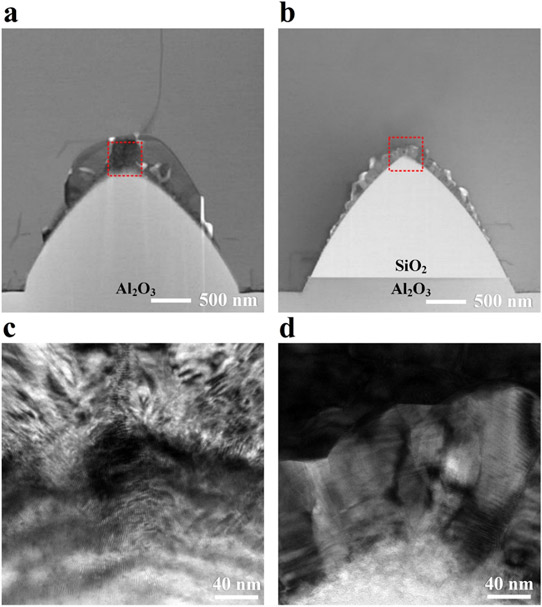
Figure 2: Cross-sectional STEM images of AlGaN grown (a) on PSS and (b) PSSA. (c) Enlarged STEM images of the marked areas in (a) and (d) that in (b).
The STEM studies also suggested that the dislocations formed at the sapphire interface became bent and terminated at the cones (Figure 2). The PSSA further reduced the upward propagation of dislocations. The PSSA sample also suffered less from parasitic crystal formation on the cones. The researchers comment: “The AlGaN epilayer grown on PSSA had a lower TDD than that grown on PSS by taking advantages of the more preferred vertical growth in the 3D growth stage and reduced misfit at the coalescence boundary.”
Under photoluminescence the peak wavelength was 368nm. Electroluminescence from the FSS, PSS and PSSA UVLEDs resulted in light output powers of 68.3, 153.8 and 193.9mW, respectively, at 150mA injection (Figure 2). The researchers attribute the enhanced performance of the PSSA device to “improved crystal quality and higher LEE”. The corresponding peak external quantum efficiencies were 23.1%, 44.9% and 50.4%. The researchers claim that the 50.4% is “better than those reported in previous publications”. The current-voltage performance of the devices was similar.
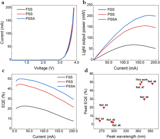
Figure 3: (a) I–V and (b) L-I characteristics of UVLEDs grown on FSS, PSS and PSSA. (c) EQEs of UVLEDs grown on FSS, PSS and PSSA versus current curves. (d) State-of-the-art in EQE for UVLEDs.
The LEE factor in the improved performance was explored using numerical simulations of the light reflection at interfaces. With the FSS substrate the flat interface tends to reflect most of the light back into the diode due to the refractive index contrasts, drastically reducing light extraction. Reflectivity measurements suggested improved reflectivity and transmittance at 368nm over FSS diodes of 10.2% for PSS devices and 15.8% for PSSA.
Patterned sapphire silica substrates UV-LEDs InGaN AlGaN MOCVD PE CVD
https://doi.org/10.1016/j.nanoen.2019.104427
The author Mike Cooke is a freelance technology journalist who has worked in the semiconductor and advanced technology sectors since 1997.


