


News: LEDs
23 January 2020
Enhancing AlGaN hole injection with germanium-doped tunnel junctions
Université Côte d’Azur and MINATEC Campus in France have used germanium (Ge) doping to improve current injection into aluminium gallium nitride (AlGaN) ultraviolet (UV) light-emitting diodes [V. Fan Arcara, J. Appl. Phys., vol126, p224503, 2019].
The Ge-doped layers were used to create the n-type side of tunnel junctions (TJs) to supply the holes for injection and recombination with electrons in quantum well (QW) light-emitting active regions. Ge doping has attracted increasing interest, compared with the more established silicon (Si).
The team comments: “Claims in favor of Ge-doping are their similar size to Ga atoms (introducing less stress in the structure than Si at high doping levels, also being compressive instead of tensile, which is the case for the latter) and the shallow behavior of its donors in GaN.”
A further advantage is that, in molecular-beam epitaxy (MBE), silicon tends to react with the ammonia (NH3) used as the nitrogen source, limiting its doping effectiveness. Ge is less prone to such reactions.
III-nitride semiconductors like AlGaN suffer from poor p-type performance since the magnesium (Mg) dopant used has a high activation energy, which increases with higher aluminium content. Even Mg-doped GaN has a poor p-type conductivity relative to many other semiconductor systems.
The AlGaN range of semiconductors have potential for UV wavelength light emission from 365nm (GaN) to 200nm (AlN). Mixed with indium (In), InGaN semiconductors are used in the visible light range (380-740nm).
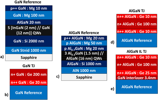
Figure 1: LED structures: (a) GaN reference (without TJ); (b) GaN TJ; (c) AlGaN reference (without TJ); (d) AlGaN TJ; (e) AlGaN IL TJ.
The researchers used metal-organic chemical vapor deposition (MOCVD) on 2-inch sapphire up to and including the last heavily-doped p++-AlGaN/GaN layer of the LED structure – i.e. the ‘reference’ sections of the devices (Figure 1).
In the MOCVD process, Si and Mg were used as n-type and p-type dopants, respectively. The light-emitting region consisted of AlGaN or InGaN QWs. After the MOCVD, the samples were annealed at 700°C for 20 minutes in nitrogen to drive out hydrogen, activating the p-type layers.
The n-type tunnel junction portions of the relevant structures were grown by molecular-beam epitaxy. The Ga and Ge came from solid sources. (Al is not mentioned, but one suspects a solid source for that metal too.) The nitrogen came from NH3.
The mesa LEDs were fabricated using reactive-ion etching and electron-beam evaporation of titanium/aluminium/nickel/gold and nickel/gold n- and p-contacts, respectively. The p-contacts of the reference devices included a 5nm/5nm semi-transparent nickel/gold layer covering the whole top of the mesa to enable better current spreading from the main 20nm/200nm p-electrode. The n-contact was rapidly annealed at 700°C in nitrogen. The semi-transparent p-contact was rapidly annealed at 450°C.
To develop the Ge-doping technology, the researchers performed calibration experiments, producing n-GaN samples with 5.5x10²⁰/cm3 carrier concentration and 67cm2/V-s mobility. These values are described as ‘state-of-the-art’. The resistivity of the material was 1.7x10⁻⁴Ω-cm.
Continuous-wave electroluminescence spectra gave peaks around 304nm and 436nm for the AlGaN and InGaN QW devices, respectively. The emissions were attributed to band-edge electron-hole recombination rather than deep-level transitions. The 304nm wavelength falls in the UV-B 280-315nm range, which has medical applications such as in the treatment of psoriasis, and is also used in the curing of photoresist layers.
In the visible 436nm-wavelength blue LEDs, the use of tunnel junctions reduced the voltage needed for a given current injection: for 100 and 500A/cm2 current densities, the GaN LEDs with and without TJs showed voltages reduced from 5.6V to 5.3V, and from 7.0V to 6.6V, respectively. The corresponding light output powers increased from 0.7mW to 0.9mW, and from 2.3mW to 2.9mW.
The researchers comment: “The slight improvement in optical power between the GaN TJ and its reference is attributed to a better transparency of the TJ-based LED since the semi-transparent Ni/Au electrode has been suppressed.”
For the AlGaN QW devices, the TJs increased the voltage for given current injection: However, inserting a GaN interlayer (IL) reduced the voltage penalty over the reference LED at 1000A/cm2 from 4.6V to 2V. The team believes that using an InGaN IL could reduce the penalty further by increasing the tunnel current, “due to a larger band-bending across the space charge region, thus decreasing the barrier width and increasing the tunneling probability”.
In terms of AlGaN QW LED optical performance, the TJ structures increased output power at 1000A/cm2 injection: 12μW for the TJ with IL, and 5.3μW without IL, compared with 1.9μW for the reference device. The team admits: “These values are low compared to the current state of the art due to the high dislocation density in the AlN buffer layer (>1010/cm2), which decreases the internal quantum efficiency (IQE) of the AlGaN/AlGaN QWs.”
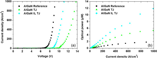
Figure 2: Current density versus bias (a) and optical power (b) for AlGaN TJs and AlGaN reference without TJ. LED areas 0.0016mm2.
The researchers believe the improved output power derives from enhanced electrical injection efficiency promoted by the use of the TJs. They comment: “As the TJ injects out of equilibrium holes into the LED, the balance between electrons and holes in the quantum wells is improved, which enhances the injection efficiency. In other words, while electrons tend to overflow above the QW in the standard UV LED due to the lack of holes and recombine in the p region, electrons recombine in the quantum wells with holes injected from the TJ in TJ-based UV LEDs.”
Germanium doping AlGaN UV LEDs MBE
https://doi.org/10.1063/1.5121379
The author Mike Cooke is a freelance technology journalist who has worked in the semiconductor and advanced technology sectors since 1997.


