


News: Optoelectronics
16 January 2020
Indium selenide expands potential of 2D optoelectronic structures
Researchers in the UK, Spain and Portugal have found that two-dimensional (2D) indium selenide (InSe) has infrared emissions that are preferentially in-plane, which could expand the capabilities of 2D optoelectronics [Mauro Brotons-Gisbert et al, Nature Communications, vol10, p3913, 2019].
The team from Heriot-Watt University in the UK, Universidad de Valencia in Spain and International Iberian Nanotechnology Laboratory (INL) in Portugal attribute the emission to excitons – bound electron-hole pairs – with a dipole moment directed out-of-plane (OP).
Other 2D semiconductors such as the transition-metal dichalcogenides (TMDs) tend to have excitons with the dipole direct in-plane (IP) with emission directed out of the plane of the semiconductor. The transition metals used include molybdenum (Mo) and tungsten (W), combined with two chalcogenide atoms such as selenium (Se) or sulfur (S). Other 2D materials with in-plane dipoles include black phosphorus and cadmium selenide.
The in-plane dipole orientation is desirable for out-coupling radiation through vertical structures. However, for in-plane photonic waveguide circuits, the out-of-plane orientation is more useful. The researchers also say that “out-of-plane dipoles present higher Purcell enhancements and couple more efficiently than in-plane ones to multimode cylindrical waveguides and optical fibers when placed in the vicinity of the waveguides.” Purcell enhancement refers to increased spontaneous emission rates due to environmental effects, such as being placed in a resonant cavity.
The 2D nature of these materials is achieved by moving from bulk material to progressively thinner layers down to a monolayer (ML). The potential for 2D optoelectronic structures arises because of strong in-plane bonding combined with weaker van der Waals bonding between layers.
The researchers comment: “The orbital nature of the electronic states at the bandgap edges makes 2D InSe a valuable building block in the design of van der Waals heterostructures with tailored optoelectronic properties. On the one hand, the strong pz orbital nature of the top valence band endows InSe with one of the largest bandgap tunability ranges found in a 2D semiconductor when its thickness varies between the bulk and the ML. On the other hand, electronic states of pz orbital nature are even under mirror symmetry operation; combining these states with the odd symmetry of the bottom of the conduction band determines the out-of-plane orientation of the luminescent excitons in this 2D semiconductor.”
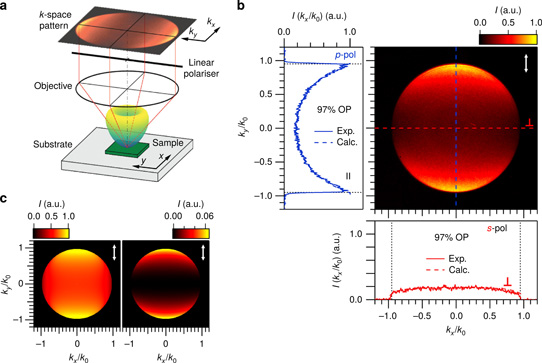
Figure 1: (a) Basic concept of k-space spectroscopy. (b) Intensity-normalized k-space emission pattern of InSe flake as function of in-plane photon wavevector normalized to that in air. Orientation of linear polarizer axis indicated by white arrow in top right corner. Blue and red solid lines in left and bottom panel show experimental k-space cross-sections in directions || and ⊥ to polarizer (and blue and red dashed lines on image, respectively). (c) Normalized emission patterns calculated for pure in-plane (left panel) and pure out-of-plane (right panel) distributions of dipoles.
Study of the polarization and directionality of the light from photoluminescence (PL) on a thick 90nm InSe layer showed exciton emissions with an out-of-plane dipole distribution of 97% (Figure 1). The substrate for the experiment was a 105nm silicon dioxide (SiO2) layer on silicon. Reducing the flake thickness to 8nm (around 10 monolayers), 2D InSe demonstrated an out-of-plane distribution of 95% (Figure 2). Compared with the 90nm flake, there was a blue-shift in the emission of 5meV from 1.244eV. The blue-shift is attributed to the 2D quantum confinement increasing the effective bandgap.
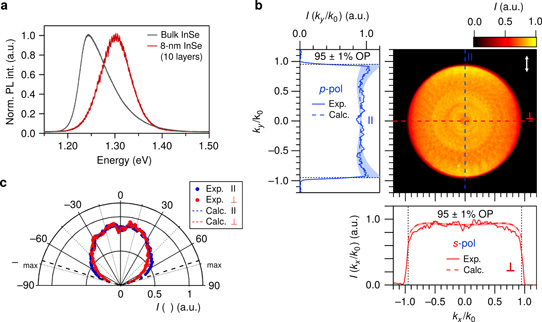
Figure 2: (a) Comparison of intensity-normalized room-temperature PL of bulk and 8nm-thick InSe. (b) Emission pattern of 8nm-thick InSe flake. (c) Measured and calculated far-field patterns as function of angle θ.
The researchers also studied MoSe2 and WSe2, since there was the possibility of ‘grey’ in-plane excitons with state splitting leading to allowed and forbidden transitions. The researchers comment: “Low-temperature PL measurements of ML WSe2 and WS2 with high NA [numerical aperture] objectives have shown that grey excitons contribute significantly to the emitted PL signal, making the low-temperature PL of these semiconductors originating not exclusively from in-plane dipoles but from a combination of in-plane and out-of-plane dipoles. However, a quantitative and unambiguous determination of the contribution of the grey excitons to the room-temperature PL of W-based TMDs is still missing.”
The team’s experimental work suggests that the in-plane contribution at room temperature is in fact 100% for WSe2.
The researchers see themselves as part of the European ‘Quantum Flagship’ project. The Valencia participants are part of the Instituto de Ciencia de Materiales (ICMUV), which is advancing a ‘Scalable Two-Dimensional Quantum Integrated Photonics’ (S2QUIP) venture with the aim of developing “circuits of quantic photonics by integrating two-dimensional semiconductor materials that are compatible with CMOS technology, often used when manufacturing traditional integrated circuits”. Such work could also lead to progress towards quantum information processing.
InSe 2D optoelectronic structures Photonics Waveguides Optical fibers
https://doi.org/10.1038/s41467-019-11920-4
www.alphagalileo.org/en-gb/Item-Display/ItemId/187007
The author Mike Cooke is a freelance technology journalist who has worked in the semiconductor and advanced technology sectors since 1997.


