


News: Optoelectronics
27 February 2020
Monolithic indium arsenide quantum dot avalanche photodiode on silicon
Researchers in the USA, China and Hong Kong have developed monolithic indium arsenide (InAs) quantum dot (QD) avalanche photodiode (APD) structures on (001) silicon (Si) with low dark current and high gain [Baile Chen et al, ACS Photonics, published online 8 January 2020].
The team from University of California Santa Barbara (UCSB) in the USA, ShanghaiTech University in China, Hong Kong University of Science and Technology, and Chinese University of Hong Kong, claim that the device is the first monolithic InAs QD APD on silicon with low dark current, which is suitable for optical fiber O-band (1260-1360nm) communications. They comment: “These QD-based APDs enjoy the benefit of sharing the same epitaxial layers and processing flow as QD lasers, which could potentially facilitate the integration with laser sources on a silicon platform.”
“When the high gain and low dark current performance up to 323K (50°C) are considered, these APDs hold great potential for applications in energy-efficient interconnects within supercomputers and data centers,” the team writes.
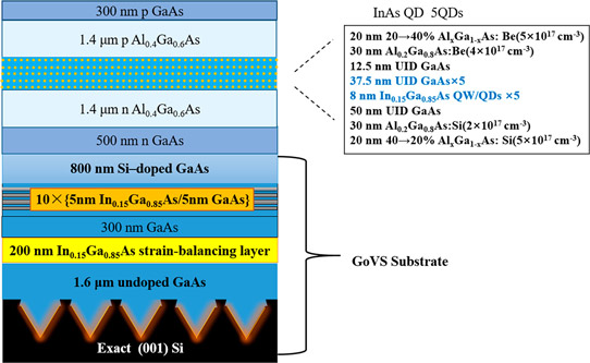
Figure 1: Schematic of InAs QD APD grown on GoVS substrate.
The substrate was gallium arsenide (GaAs)-on-V-grooved-Si (GoVS) produced using metal-organic chemical vapor deposition (MOCVD) – see Figure 1. The grooves in the (001) Si enabled the reduction of threading dislocations through aspect ratio trapping (ART). Further growth used molecular beam epitaxy (MBE) to produce a dot-in-well (DWELL) structure. The QDs consisted of a 5-layer stack. The final dot density was 6x10¹⁰/cm2. The barrier matrix for the dots and the well barriers consisted of aluminium gallium arsenide (AlGaAs).
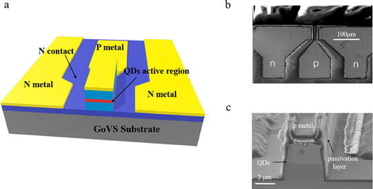
Figure 2: (a) Schematic of fabricated waveguide photodetector. (b) Top-view and (c) cross-sectional scanning electron microscope views.
APD fabrication created waveguide-shaped devices (Figure 2). The mesas were etched with inductively coupled plasma. Sidewall passivation consisted of 12nm atomic layer deposition (ALD) aluminium oxide (Al2O3) and 1μm silicon dioxide (SiO2) to suppress current leakage. The metal contacts were palladium/titanium/palladium/gold and palladium/germanium/palladium/gold. The structure included standard 150μm-pitch ground-signal-ground (GSG) pads. The devices were cleaved to produce optical entry facets without anti-reflective coatings.
The room-temperature (300K) dark current for a 3μmx50μm device was 0.1nA (6.6x10⁻⁵A/cm2) under -5V bias. The researchers attribute the low value to high crystal quality and good surface passivation of the mesa sidewalls. With the APD near breakdown (99%), the dark current was 1.3nA at -15.9V bias. An increase in breakdown voltage with temperature indicated to the team that avalanche rather than tunneling was the main mechanism. The parasitic capacitance of the device was 517fF at room temperature.
The peak avalanche gain for 1300nm-wavelength light was 198 at 293K (20°C), relative to the ‘unity gain’ performance at -5V bias. The peak reverse bias was -15.97V. The dark current at that bias was 33nA. The peak gain reduced to 73 at 323K (50°C).
The researchers note that the 33nA dark current value is “more than two orders of magnitude lower than that of Si/Ge APDs, InGaAs/InAlAs APDs on Si, and the recent InAs QD APDs heterogeneously integrated on Si”.
Noise was a problem with the device – the excess noise figure reached more than 60 with the gain at 8. The researchers comment: “The excess noise is high due to the mixed injection in the APD device, and further optimization for minimizing the noise performance is necessary for future work.” The team also suggests that one way to overcome this would be to use separated absorption, charge, and multiplication avalanche photodiode (SACM-APD) structures, aiming at low noise and high speed.
The response to 1310nm light input (-20dBm power) was 0.234A/W with -5V bias. The response cut off at around 1360nm, corresponding to the approximate bandgap of the InAs QDs. With the reverse bias at -15.9V, the response was 4.8A/W at 1310nm, representing an avalanche gain of about 20. The cut-off wavelength red-shifted at the increased reverse bias due to quantum-confined Stark effects - “which shifts the electron states to lower energies and the hole states to higher energies, respectively, in the QD layers,” as the team puts it.
The response to modulated signals showed a 3dB bandwidth of 2.26GHz with the bias at -6V, reducing to 2.06GHz at -15.9V. The researchers attribute the reduction to avalanche build-up time at the higher reverse bias. The resistance-capacitance (RC)-limited bandwidth was estimated at 5.16GHz. The researchers plan to look at improving the RC performance using semi-insulating silicon substrates or thick benzocyclobutene (BCB)/SU8 layers to reduce parasitic capacitance effects.
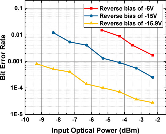
Figure 3: BER versus input optical power.
The performance with pseudorandom binary sequence modulation at -3dBm power produced ‘open-eye’ diagrams up to 8Gbit/s data rates. With 2.5Gbit/s sequences the bit-error rate (BER) was significantly reduced at -15.9V bias (two orders of magnitude relative to -5V, Figure 3).
Monolithic InAs quantum dot avalanche photodiode InAs APD GoVS substrate MOCVD AlGaAs
https://dx.doi.org/10.1021/acsphotonics.9b01709
The author Mike Cooke is a freelance technology journalist who has worked in the semiconductor and advanced technology sectors since 1997.


