


News: Microelectronics
13 February 2020
Probing vertical conduction in indium selenide field-effect transistors
Northwestern University in the USA reports on its recent work probing the conduction properties of indium selenide (InSe) vertical field-effect transistors [Vinod K. Sangwan et al, Appl. Phys. Lett., vol115, p243104, 2019].
InSe is a recent addition to the stable of two-dimensional (2D) materials where the crystal structure consists of relatively easily separated layers. This results from an atomic lattice with strong in-plane bonds with weak ‘van der Waals’ bonds between the layers. Initial studies have tended to focus on lateral in-plane properties in terms of electron conduction. The electron mobility can be more than 1000cm2/V-s.
The Northwestern researchers comment: “By elucidating fundamental vertical charge transport mechanisms in InSe, this work provides guidance to ongoing efforts to employ InSe in vertical heterostructures, photovoltaics, photodetectors and related vertical device technologies.”
A Europe-based research group has recently found that the excitons in InSe tend to have out-of-plane dipoles, which may be useful for coupling in-plane photons into waveguide structures and optical fibers [Mauro Brotons-Gisbert et al, Nature Communications, vol10, p3913, 2019, news story at www.semiconductor-today.com/news_items/2020/jan/heriotwatt-160120.shtml].
The devices used a silicon back-gate configuration with the 2D layers manipulated on an oxidized layer of silicon dioxide (SiO2, Figure 1). The InSe was positioned on patterned graphene. The top drain electrode consisted of chromium/gold (Cr/Au), which gives an ohmic contact with InSe. The graphene layer provided the grounded source.
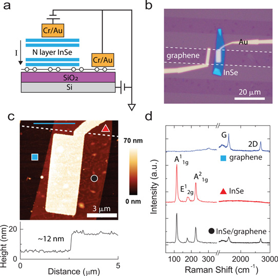
Figure 1: (a) Schematic of graphene-InSe vertical field-effect transistor (VFET) on oxidized silicon substrate. (b) Optical image where white dashed lines show etched graphene stripes. (c) Atomic force microscopy topography image (top). Height profile (solid blue line) shows 12nm InSe flake thickness (bottom). White dashed line marks graphene edge. (d) Raman spectral peaks for graphene (blue square in (c)), InSe (red triangle), and combined InSe/graphene (black circle) regions.
The InSe flakes were mechanically exfoliated from material supplied by American Elements Corp. Mechanical exfoliation describes the creation of flakes of material by application of sticky Scotch tape.
The materials were handled in an inert nitrogen environment to avoid performance degradation from surface contamination and so on. Measurements were made in vacuum conditions with the pressure at less than 5x10⁻⁵Torr. Some 14 samples were studied with InSe thickness ranging from 9.5nm up to 43nm.
With the drain positively biased, the graphene/InSe interface was found to have a reverse-biased Schottky barrier. The silicon back-gate modulated current flow through the barrier. The InSe was found to be unintentionally n-type in conduction behavior.
The maximum/minimum on/off current (ION/IOFF) ‘switching’ ratio increased by a factor of 50 as the InSe thickness increased from 9.5nm to 43nm. This increase is attributed to a higher Schottky barrier in the contact between graphene and the thicker material, reducing the off-current leakage.
The on-current density was of the order 5-10 down on what is found in black phosphorus VFETs. The researchers explain: “Black phosphorus has a smaller bandgap (~0.3eV in bulk), higher intrinsic doping, and an out-of-plane electron lone pair in phosphorus, which enhance out-of-plane conductivity.” The bulk bandgap of InSe is ~1.25eV.
The InSe switching ratio was ~104 for thicker layers, while that of comparable black phosphorus devices is ~50. The transition-metal dichalcogenide tungsten diselenide (WSe2) gives switching of more than 106.
Reducing the device temperature from 295K to 190K resulted in an increase in the switching ratio by a factor of around six. While there was a decrease in conductivity at the lower temperature, there was also a more rapid decrease in off-current leakage.
There was a larger conductivity variability in thicker InSe flakes – this suggests a more thermionic emission behavior with hot electrons crossing above the barrier rather than Fowler-Nordheim tunneling through the barrier. By contrast, devices with thinner InSe layers showed a relatively constant Schottky barrier height of ~100meV. The thick InSe VFETs had about a two-fold increase in extracted Schottky barrier height at room temperature, relative to 190K.
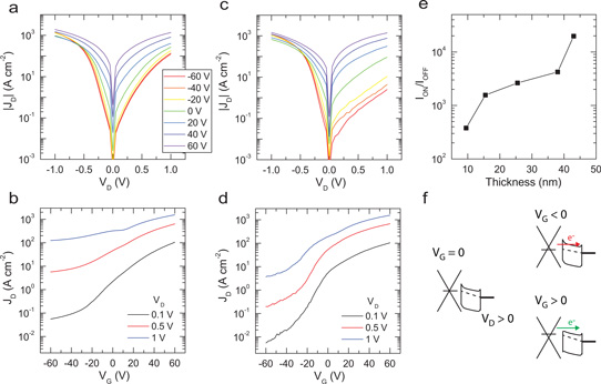
Figure 2: Room-temperature charge transport characteristics of InSe VFETs. (a) Current density (JD) versus drain voltage (VD) output characteristics of thin InSe VFET. (b) JD versus gate voltage (VG) transfer characteristics of thin InSe VFET at different VD values. (c) Output characteristics of thick InSe VFET. (d) Transfer characteristics of thick InSe VFET. (e) ION/IOFF switching ratio versus InSe thickness. (f) Schematic band diagrams of InSe VFET with zero, negative, and positive back-gate bias.
The analysis led the researchers to attribute an out-of-plane effective mass of 2.57x that of a free electron at 190K. Previous cyclotron resonance and optical absorption measurements gave values in bulk InSe ranging from 0.25x (20K) to 34.3x (200K), respectively. The team comments: “Layered materials often show large anisotropy of the effective mass and carrier mobility (µ), which results in InSe VFETs possessing intrinsically weaker out-of-plane transport (μ⊥/μ∥ = 0.002 for InSe).” The researchers also point out that the 2.57x value “is substantially higher than the in-plane effective mass.” They do not provide a comparison figure for the latter.
InSe vertical field-effect transistors InSe VFET
https://doi.org/10.1063/1.5128808
www.americanelements.com/indium-selenide-crystal-12056-07-4
The author Mike Cooke is a freelance technology journalist who has worked in the semiconductor and advanced technology sectors since 1997.


