


News: Microelectronics
6 February 2020
Developing complementary p-channel transistors for GaN-on-silicon power
Hong Kong University of Science and Technology (HKUST) report on p-channel metal-oxide-semiconductor field-effect transistors (MOSFETs) produced on gallium nitride (GaN) on silicon (Si) substrates [Zheyang Zheng et al, IEEE Electron Device Letters, vol.41, p26, 2020]. The researchers used commercial 8-inch-diameter GaN-on-Si wafers with epitaxial structures designed for 650V normally-off p-GaN gate power high-electron-mobility transistors (HEMTs) (Figure 1).
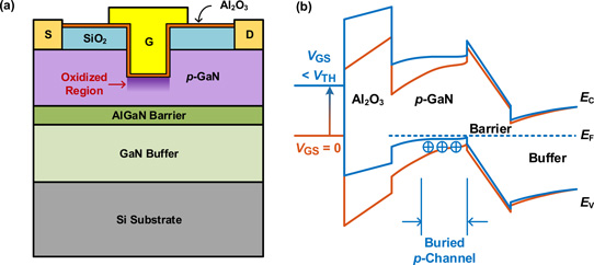
Figure 1: Schematic of (a) E-mode GaN pFET (LGS/LG/LGD = 4/2/4μm) and (b) energy band diagram at gated region of buried p-channel with 0V (OFF) and beyond threshold (ON) gate potentials (VGS).
GaN is being developed for high voltage and power handling based on the material’s high critical electric field before breakdown. Devices with n-type channels with negatively charged carriers (electrons) have been intensively developed in recent years. Much progress has been made in developing devices with normally-off ‘enhancement-mode’ (E-mode) characteristics, rather than the more easily achieved normally-on ‘depletion-mode’ (D-mode). The E-mode is desired for lower power consumption and for fail-safe features.
The n-channel devices largely depend on the creation of ‘two-dimensional electron gas’ (2DEG) channels, which arise near the interface between GaN and a barrier layer, often aluminium gallium nitride (AlGaN). The 2DEG occurs due to band-bending effects arising from contrasts in the charge distribution in the chemical bonds holding the Ga, Al and N atoms together.
Devices with p-channels would enable complementary integrated circuit (IC) designs, which would further reduce power loss in logic control systems. Although some progress has recently been made in developing an analogous 2D hole gas for p-channels, effective devices remain to be achieved. The HKUST work focuses instead on using p-GaN material achieved using magnesium doping.
The team comments: “The p-GaN/AlGaN/GaN-on-Si platform paves the way to monolithically integrating E-mode pFET and nFET for possible GaN complementary and more robust GaN power ICs.”
The GaN-on-Si material included a ~12nm AlGaN barrier and a ~85nm p-GaN top layer. The undoped GaN buffer was ~4.5µm thick. The structure was found to have a hole sheet density of 1.23x10¹³/cm2 and mobility 10.2cm2/V-s, according to Hall measurements.
Standard p-GaN gate E-mode n-channel HEMTs realized on the substrate typically have threshold voltages of +1.7V and an on-current of 350mA/mm with 5V drain bias. The on/off current ratio is usually of order 109.
The HKUST p-channel devices were fabricated with 500°C-annealed nickel/gold ohmic source-drain (S-D) contacts evaporated onto the p-GaN, which had previously been subjected to a 5-minute buffered oxide etch, presumably to improve the surface and remove contaminants.
The gate (G) recess was defined by a 200nm plasma-enhanced chemical vapor deposition (PECVD) silicon dioxide (SiO2) hard mask, which also served as surface passivation. The p-GaN recess was formed using inductively coupled plasma reactive-ion etch.
An oxygen plasma treatment increased the surface roughness at the bottom of the recess from 0.36nm root-mean-square to 0.41nm, according to atomic force microscopy. The recess depth was found to be about 54nm, leaving ~31nm of p-GaN material above the AlGaN barrier for the channel.
The gate structure was completed with 20nm atomic layer deposition (ALD) aluminium oxide (Al2O3) insulation and 400°C-annealed nickel/gold metal electrode. The electrical isolation of the devices was from fluorine ion implantation rather than mesa etching. The researchers used fluorine implant to avoid current leakage along rough mesa sidewalls. The implant occurred between the Al2O3 and gate metal deposition steps.
The device demonstrated a threshold voltage of -1.7V, giving normally-off enhancement-mode behavior at 0V gate. The oxygen plasma treatment enabled the negative threshold – without the treatment, the device became depletion-mode (normally-on at 0V gate) with the threshold at +2.2V. The on-current of the enhancement-mode device was 67% that of the depletion-mode transistor without oxygen plasma treatment.
The on-resistance for the E-mode device was a “relatively large” 2.4kΩ-mm at low drain bias. This reduced somewhat at -5V drain to 1.6kΩ-mm. The maximum drain current was 6.1mA/mm at -10V drain. The off-current with 0V gate was 1.2x10⁻⁷mA/mm. The team sees this low off-current as “delivering an ultra-low static power consumption required in CMOS logic gates.”
The researchers explain the action of the oxygen plasma treatment: “It is known that oxygen induced into p-GaN could either behave as shallow donors to compensate the Mg acceptors or form inert Mg-O complexes to de-activate the Mg acceptors, both of which would result in depletion of holes. Hence, it is plausible to assume that the top oxidized GaN has its Mg doping compensated and the energy band bent downward to form a hole barrier that buries the p-GaN channel away from the top GaN surface.”
The downward band bending pushes the depletion region under the recessed gate to extend through the p-GaN layer, reaching the AlGaN barrier. This enables enhancement-mode operation by turning off the buried p-channel at 0V gate potential.
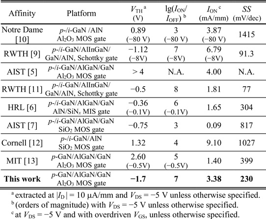
Table 1: Benchmark of p-channel GaN FETs.
The researchers compared their device with others previously presented in the scientific literature (Table 1). The team comments: “Among all the p-channel GaN MOS-FETs, the one from this work exhibits the combination of high ION, high ION/IOFF, the lowest subthreshold swing (SS) and E-mode operation. Devices implemented on the platform with quaternary back-barrier and Schottky gate exhibit outstanding SS and ION, but suffers large gate leakage at the ON state.”
GaN-on-silicon MOSFET HEMT AlGaN GaN
https://doi.org/10.1109/LED.2019.2954035
The author Mike Cooke is a freelance technology journalist who has worked in the semiconductor and advanced technology sectors since 1997.


