


News: Optoelectronics
3 December 2020
CW quantum dash lasers on silicon
Hong Kong University of Science and Technology (HKUST) in China claims the first continuous wave (CW) C-band (~1580nm wavelength) quantum dash (QDash) laser diodes on planar silicon with threshold current densities as low as 1.55kA/cm2 [Wei Luo et al, Photonics Research, vol8, p1888, 2020].
The researchers see “great potential as critical components in high-volume, low-cost integrated silicon photonics circuits”. The team also suggest that the QDash format could be used in semiconductor optical amplifiers, modulators and photodetectors. Apart from high-speed/high-capacity data transmission, such devices could be deployed as light detection & ranging (LiDAR) components.
The use of low-cost silicon in the orientation favored for CMOS (001) could open up wider deployment, particularly with a monolithic growth process that can avoid the potential for defects from the relatively high 8% lattice mismatch between silicon and indium phosphide (InP). The use of quantum dots or dashes mitigates this to some extent, but further defect reduction is needed for effective laser or other light-emitting and -detecting structures.
The growth was through metal-organic chemical vapor deposition (MOCVD) on nominal (001) Si. In-house measurement determined the offcut angle at 0.5° along the [110] direction. A number of growth steps were implemented to counteract the various defect formation mechanisms.
First the silicon substrate was subjected to a 800°C anneal in hydrogen. According to the team, this helps to avoid anti-phase boundary formation through desorbing oxides and rearranging the surface atoms.
The first buffer layer was 1μm of gallium arsenide (GaAs), grown as an intermediate layer between the planar silicon and InP lattices in three temperature steps: 400°C, 500°C and finally 600°C. The defect density in this buffer was reduced by using a five-stage thermal anneal cycling between 330°C and 780°C, reducing the x-ray diffraction (XRD) rocking curve full-width at half-maximum (FWHM) from 580arcsec to 380arcsec. The root mean square (RMS) surface roughness of the GaAs on planar Si (GoPS) was 1.1nm in atomic force microscopic analysis of a 10μmx10μm field.
The 3.1μm InP buffer was grown in three steps also: 445°C, 555°C and 630°C. The InP grown at the highest temperature included three 10-period 11.5nm/31nm In0.63Ga0.37As/InP superlattice structures designed to filter out threading dislocations. The InP spacers between the superlattices were 250nm thick. The 2.8nm RMS surface roughness was somewhat larger than for the GaAs surface. Transmission electron microscope (TEM) analysis of the surface gave an estimate for the defect density at 3.6x10⁸/cm2 with 0.4x10⁸/cm2 standard deviation.
Various QDash structures (Figure 1) were grown on this material. The QDashes themselves were assembled from an InAs layer on strained InGaAs. A series of ‘dot-in-well’ (DWELL) QDash layers were grown using InGaAs and/or InAlGaAs capping in low- and high-temperature steps.
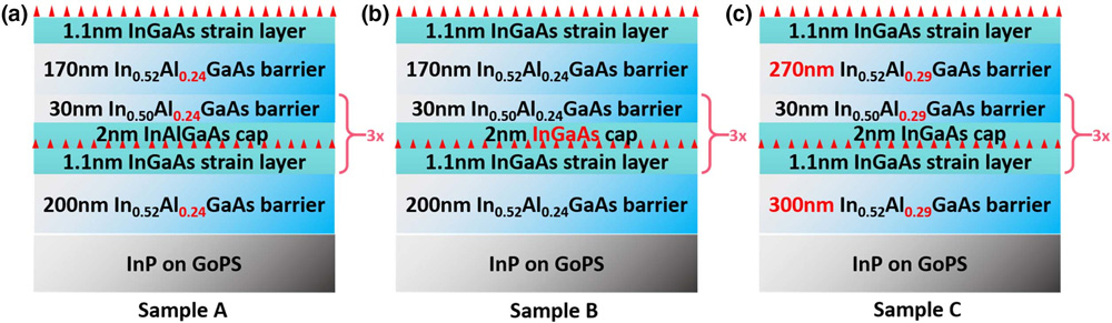
Figure 1: Schematic sample variations of QDash structures grown on InP/GoPS with different structures.
The QDash DWELLs were sandwiched between separate-confinement heterostructures: InAlGaAs cladding lattice-matched to the InP template. The 30nm InAlGaAs spacer layer was slightly strained, compensating for the accumulated strain from the QDashes. A final QDash layer was grown on the surface to enable easy material analysis.
Three different samples were produced in an effort to determine the optimum optical confinement from the cladding, varying the refractive index contrast and layer thickness. The QDashes were found to be elongated along the [1-10] direction. The dot density was 3.5x10¹⁰/cm2. The highest photoluminescence intensity was from sample B, which used an InGaAs cap, reducing the energy gap between the well and QDashes.
The researchers comment: “The elimination of aluminium in the cap layer helps to reduce the impurities, which accounts for the increased PL intensity in Sample B. In addition, by changing the low-temperature cap layer with little composition difference, the local strain of QDashes is also modified, which influences the morphology and emitting wavelength of QDashes”.
The lower aluminium content of the InAlGaAs barriers in sample B also reduced the bandgap and increased the refractive index relative to sample C. This should lead to improved optical confinement, but the reduced bandgap could risk reduced carrier confinement in the DWELL layers.
For electrically pumped lasers the growth sequence was 600nm n-InP contact, 630nm n-InP cladding, three-stack QDash active region, 1500nm p-InP cladding, and 140nm p-InGaAs contact.
The three types of QDash structure were used in ridge-waveguide laser diodes with a first mesa terminating just above the active region and a second at the n-InP contact layer. The samples were thinned to 100μm before cleaving into laser bars. The facets were not coated.
The turn-on voltage in pulsed testing was around 0.7V for all the devices. Laser diodes based on sample A would not lase in continuous wave (CW) operation. Again, sample B gave the best performance in terms of low threshold current, and in terms of operation to the highest temperature of 90°C. The characteristic temperature (T0), reflecting slower variation in threshold, was also higher in sample B laser diodes under pulsed conditions.
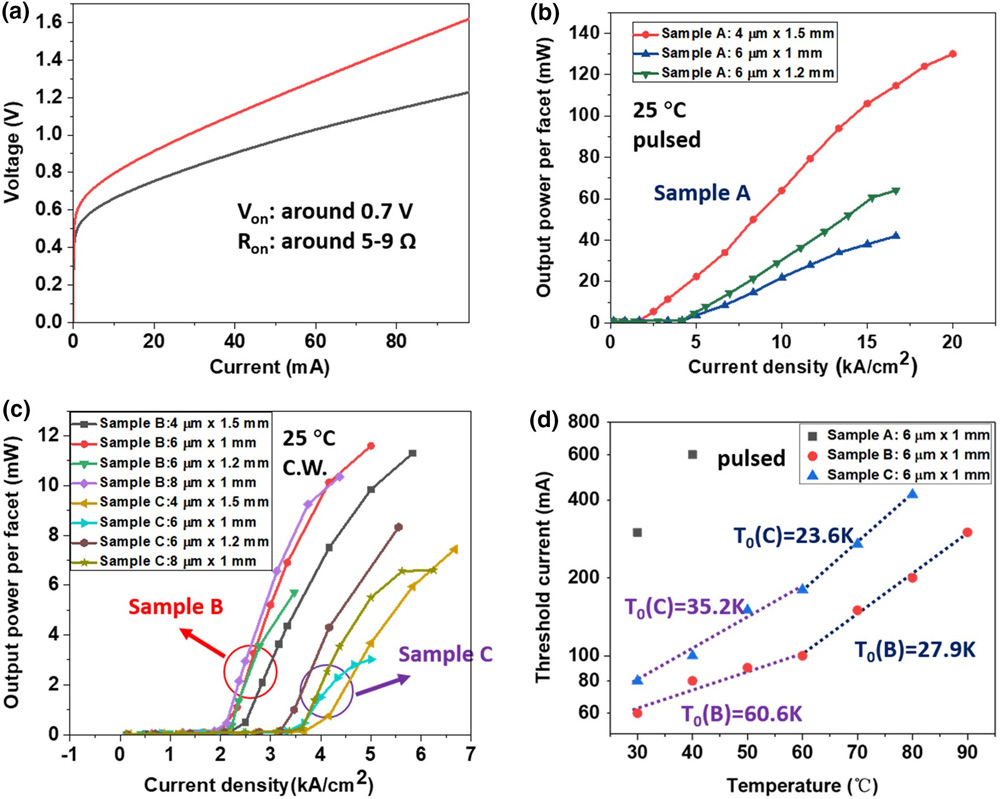
Figure 2: (a) Representative current-voltage curves of fabricated devices. (b) Room-temperature pulsed lasing light output power-current density (L-I) curves of different size FP lasers on Sample A. (c) Room-temperature CW lasing L-I curves on Samples B and C. (d) Pulsed lasing threshold currents of 6μmx1mm lasers on Samples A, B and C at different temperatures.
The researchers comment: “Compared to the characteristic temperature T0 of QD laser on native InP substrate, the smaller T0 value here may be caused by the imperfect InP-on-Si buffer quality, which introduces the non-radiative recombination centers in the active region.”
A variation of the laser diode structure with the ridge created in one step down to the n-InP contact enabled a reduction of the threshold current density to 1.55kA/cm2 in CW operation in a 8μmx1.5mm device. The single-facet output power was as high as 14mW. The emission spectrum consisted of multiple peaks, centered on 1580nm, due to the large size of the cavity, supporting a number of Fabry-Perot modes. The laser diode continued lasing up to 95°C under pulsed operation.
CW quantum dash laser InP GaAs MOCVD Silicon substrate InGaAs InAlGaAs
https://doi.org/10.1364/PRJ.403938
The author Mike Cooke is a freelance technology journalist who has worked in the semiconductor and advanced technology sectors since 1997.


