


News: Optoelectronics
14 August 2020
Gallium nitride VCSEL with electrically conductive bottom mirror and contact
Researchers based in the USA and South Korea claim the first electrically injected III-nitride vertical-cavity surface-emitting laser (VCSEL) using an electrically conductive distributed Bragg reflector (DBR) containing nanoporous (NP) gallium nitride (GaN) [Rami T. ElAfandy et al, Appl. Phys. Lett., vol117, p011101, 2020].
The team from Yale University in the USA and Sunchon National University in South Korea hope that their work will help overcome the limitations of present attempts at producing blue and ultraviolet VCSELs from III-nitride materials with similar performance to those produced for infrared and longer visible wavelengths.
The team sees the “main bottleneck” as being the bottom DBR needed for forming the vertical cavity that confines the optical field. Yale reported its electro-chemical technique for creating porous GaN in 2010. The porous material has a tunable refractive index, allowing the creation of a DBR structure. The researchers have produced m-plane GaN VCSELs using the technology, reported in 2019, but an intracavity was used, rather than a bottom contact, because the DBR was too resistive. The new c-plane structure allows a bottom-contact operation.
The team reports: “The present studies demonstrate that the conductive nanoporous GaN DBR can potentially fulfill all the requirements for the VCSEL operation and offer a unique pathway for scalable and controllable mass production.”
Some of the Yale research money came from IP Group Inc, a fund for investors in R&D.
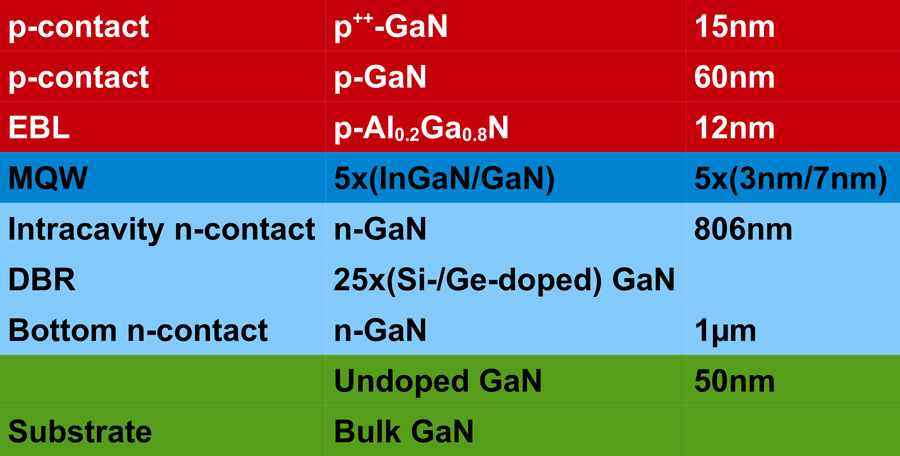
Figure 1: Epitaxial material with indium gallium nitride (InGaN) multiple quantum wells (MQWs) and aluminium gallium nitride (AlGaN) electron-blocking layer (EBL).
The epitaxial material was grown on 2-inch c-plane bulk GaN substrate, offcut 0.35° in the m-direction (Figure 1). The bottom DBR material consisted of layers alternately doped with silicon (Si) and germanium (Ge) with concentrations of 5x10¹⁸/cm3 and 6x10¹⁹/cm3, respectively. The epitaxial structure was annealed at 800°C in nitrogen for 20 minutes in the metal-organic chemical vapor deposition (MOCVD) reactor to activate the magnesium doping of the p-contact layers. The cavity was designed to be six wavelengths (6λ) long.
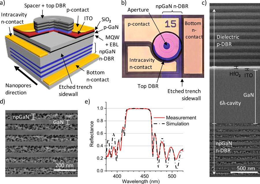
Figure 2: (a) Schematic representation and (b) top-view optical image of nanoporous GaN blue VCSEL. (c) Cross-sectional scanning electron micrograph (SEM) of full VCSEL device. (d) Cross-sectional SEM and (e) reflection spectrum (measured, red; simulated, black) of nanoporous GaN DBR.
Inductively coupled plasma etching was used to create platforms for intracavity (150nm deep) and bottom (3.5μm deep) n-contacts, and to expose the DBR material for the porosification process with nitric acid coupled with a 1.6V bias (Figure 2).
The p-contact structure consisted of 30nm silicon dioxide (SiO2), defining the current aperture, and 30nm indium tin oxide (ITO) for current spreading. The contact metal stacks consisted of titanium/aluminium/nickel/gold. The top reflector was a dielectric structure consisting of 40nm hafnium dioxide (HfO2) spacer, and SiO2/HfO2 DBR pairs.
Using calibration structures before producing the VCSEL, the researchers determined the stop gap of the bottom DBR at 39nm for more than 98% reflection, and peak reflectance of 99.6%. The team reports: “This stop band is at least two times wider than the previously reported epitaxial DBRs, with a uniformity of <2nm shift in the center wavelength across a 2” wafer.” The nanoporous GaN had a refractive index of 2.06, according to a fit using the transfer matrix method.
The VCSELs were tested using 200ns pulse current injection with 0.4% duty cycle. With intracavity injection, the turn-on voltage was 5.4V and the laser threshold came at 42kA/cm2 current density (Figure 3). The maximum light output power was 0.17mW at 78kA/cm2. The peak wavelength was 434nm.
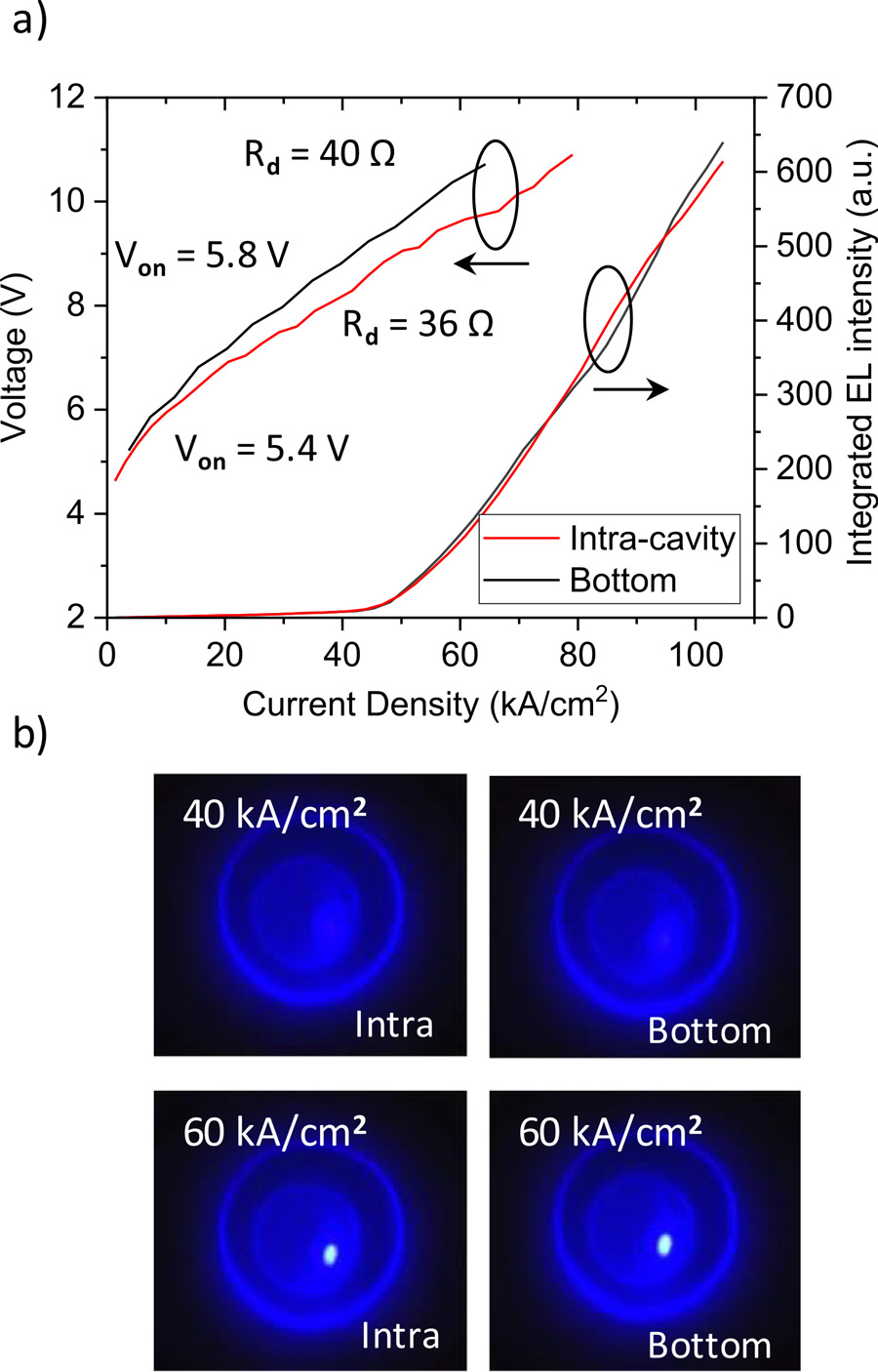
Figure 3: (a) Voltage and light output power versus current density of nanoporous GaN VCSEL through intracavity (red) and bottom (black) injection. (b) Near-field images of aperture below (40kA/cm2) and above (60kA/cm2) lasing threshold from intracavity (left) and bottom (right) injection.
Inspection of the laser output showed bright spots, associated with filamentary laser structures in the device. The light output power had kink increases at 54kA/cm2 and 74kA/cm2, which were attributed to additional filaments beginning its lase.
Using the bottom contact increased the turn on voltage by 0.4V. The threshold current and light output power performance with respect to current injection showed “no observable difference”, according to the researchers. Visual inspection of the output showed similar emission patterns and filamentation.
The team comments: “This study establishes the bottom contact as a viable and efficient current injection scheme for the nanoporous GaN VCSELs, bringing the III-nitride VCSELs closer to technological feasibility.”
The threshold was rather high, so the researchers examined the material under a phase-contrast optical microscope. They found undulations, which they believe to be due to step-bunching occurring during the growth process as a result of heavy doping in the bottom DBR layers. The team comments: “These grown-in surface undulations can impact regions including DBR mirror, InGaN quantum wells, and the p-type doping.”
VCSEL DBR GaN Nanoporous GaN InGaN AlGaN MOCVD
https://doi.org/10.1063/5.0012281
The author Mike Cooke is a freelance technology journalist who has worked in the semiconductor and advanced technology sectors since 1997.


