


News: Optoelectronics
20 August 2020
Boron strain therapy for high-indium-content InGaAs layers
University of Texas at Austin in the USA has claimed the longest photoluminescence (PL) wavelength achieved so far of 1.4μm in the near infrared (NIR) for boron gallium indium arsenide (BGaInAs) along with electroluminescence (EL) experiments emitting close to the same wavelength region [R. H. El-Jaroudi, Appl. Phys. Lett., vol117, p021102, 2020]. The 1.3μm wavelength is particularly interesting for fiber-optic data transmission, along with light detection & ranging (LiDAR) and face-recognition technologies.
Vertical-cavity surface-emitting lasers (VCSELs) and related devices are a much desired technology for this range, but are limited in performance due to the difficulty in producing suitable light-emitting active layers.
A particular problem is that high-indium-content InGaAs is compressively strained relative to the surrounding GaAs and aluminium gallium arsenide (AlGaAs) used to achieve carrier injection and distributed Bragg reflectors (DBRs), along with the GaAs substrate base.
Attempts have been made to modify the InGaAs layer to reduce strain effects such as using quantum dots or nitrogen incorporation (InGaNAs). The quantum dot approach suffers from low modulation bandwidth, and nitrogen substitution is hard to achieve effectively.
The Texas/Austin team comments: “The advantage of dilute borides over the dilute nitrides is a predicted higher solid solubility of boron than nitrogen, enabling higher incorporation and simplified growth of dilute-boride alloys compared to nitride alloys.”
However, boron-V semiconductors (‘boron pnictides’) are also difficult to realize, since they have higher melting points than other compounds in the III-V family. Up to now, demonstrated BGaInAs PL emission has peaked at less than 1.2μm wavelength.
The researchers used solid-source molecular beam epitaxy (MBE) to produce BGaInAs heterostructures on (100) on-axis semi-insulating GaAs substrate at 380°C. The arsenic flux came from a valved cracker system. The gallium and indium were produced by effusion cells.
The boron was evaporated using an electron-beam system with the flux controlled by the input power. One drawback of this was that it inhibited the use of reflection high-energy electron diffraction (RHEED) for in-situ process monitoring. However, when the boron flux was completed, the researchers did observe the hoped-for ‘streaky’ RHEED patterns indicative of a two-dimensional growth mode.
Samples for photoluminescence (PL) study consisted of 200nm GaAs buffer, 10nm (B)GaInAs quantum well (QW), and 50nm GaAs cap. The process conditions were determined through a series of calibration experiments involving InGaAs/GaAs superlattices and BGaAs films.
The researchers grew QWs with more than 40% indium which, without boron, suffered from complete suppression of PL. This was attributed to a high compressive strain of -3%. The introduction of between 2% and 6% boron compensated the compression, giving strain values nearer 0%: -2.7% and -2.1%, respectively, according to x-ray analysis.
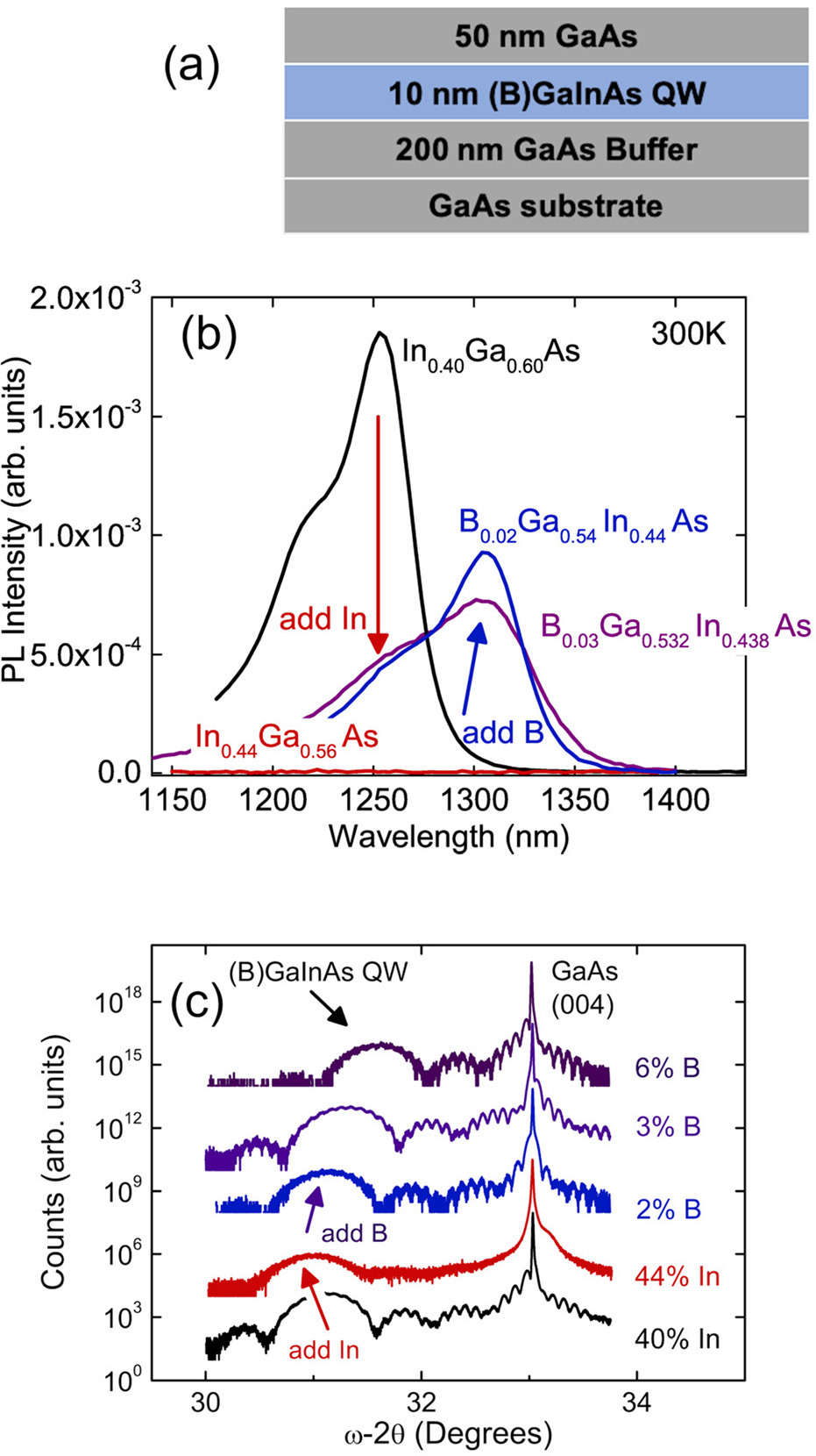
Figure 1: (a) Layer structure of (B)GaInAs PL samples. (b) PL of the (B)GaInAs QWs on GaAs, targeting 1.3μm. (c) High-resolution x-ray diffraction (HR-XRD) of (B)GaInAs QWs on GaAs.
The incorporation of 2% boron enabled optical quality to be improved, as evidenced by recovery of finite thickness fringes in the x-ray analysis and increased PL intensity (Figure 1). By contrast, the incorporation of 1% nitrogen has been found to severely reduce InGaNAs optical quality at 1.3μm target wavelengths.
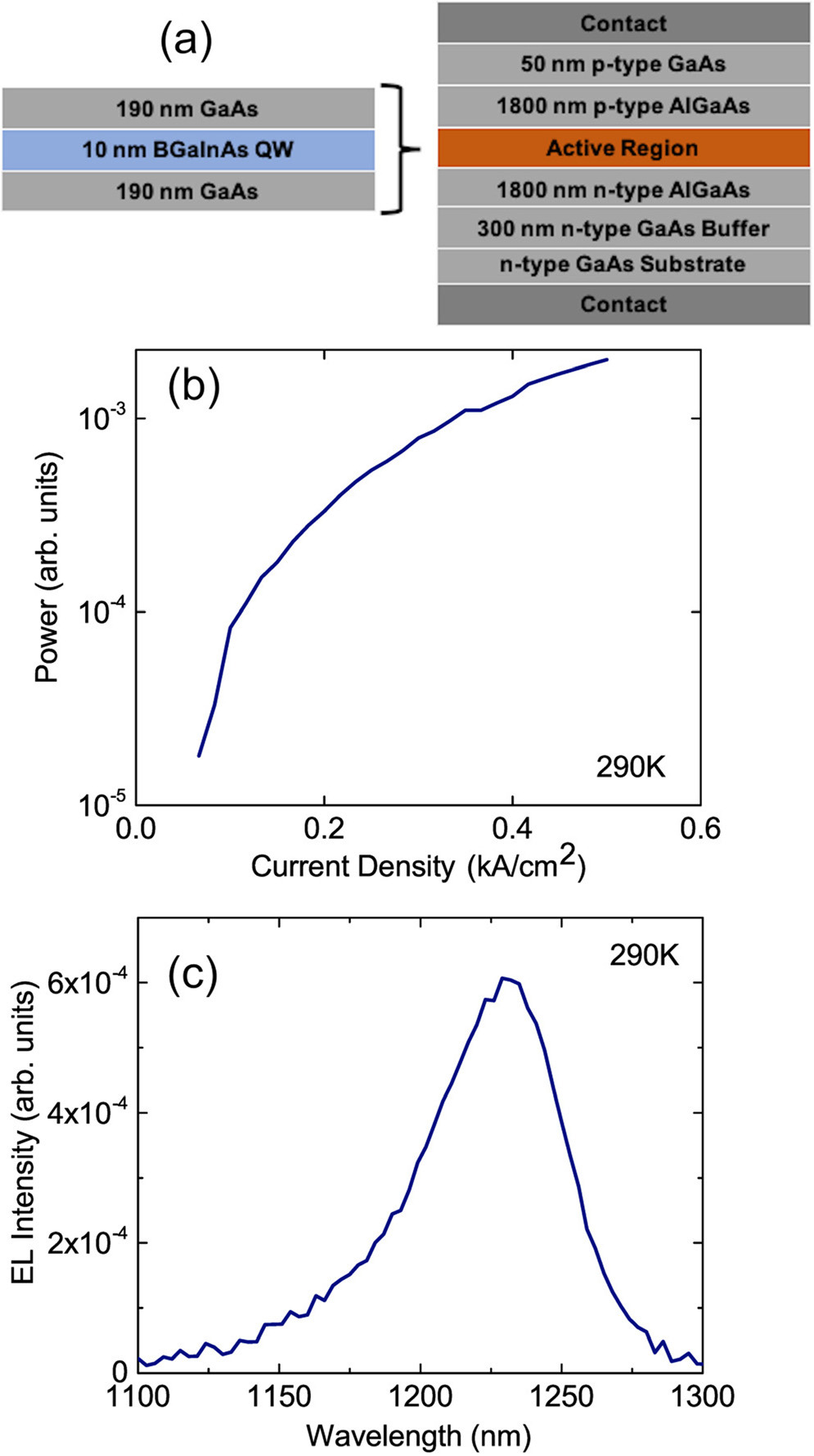
Figure 2: (a) EL structure with BGaInAs QW active region. (b) Light output versus input current (L-I) curve and (c) emission spectrum at 0.5kA/cm2 current density.
The team also produced an electoluminescence (EL) structures with B0.02Ga0.54In0.44As QW active light-emission region (Figure 2). Aluminium gallium arsenide (AlGaAs) grown at 580°C was used for the p- and n-type carrier injection. The substrate was (100) n-GaAs. The n- and p-type dopants were silicon and beryllium, respectively. Although the BInGaAs was produced under the same conditions as the PL sample, the EL emission peak was at a shorter wavelength of less than 1.25μm. The device was operated in pulsed mode.
The researchers studied the effect of ex-situ annealing in the range 550-700°C, suggesting that the blue-shift in the EL device was due to an in-situ annealling effect on the QW from the high temperature needed for AlGaAs MBE. The ex-situ annealing was indeed found to cause a blue-shift in PL studies. With InGaNAs, such a blue-shift from annealing has been attributed to rearrangement of In-N nearest neighbors.
A PL sample with B0.05Ga0.45In0.50As QW annealed at 700°C for 1 minute had an emission peak at 1.3μm. The annealing also increased the PL intensity relative to an unannealed sample. Without annealing, the QW emitted around 1.4μm.
https://doi.org/10.1063/5.0011147
The author Mike Cooke is a freelance technology journalist who has worked in the semiconductor and advanced technology sectors since 1997.


