


News: Microelectronics
19 August 2020
Avoiding mobility collapse in high-voltage gallium nitride power devices
Japan’s SCIOCS Co Ltd has claimed the highest mobility achieved at room temperature for n-type gallium nitride (n-GaN) with low carrier density of the order of 1015/cm3 [Hajime Fujikura et al, Appl. Phys. Lett., vol117, p012103, 2020]. Such low-doping layers are key components of vertical power devices with voltage ratings up to 10kV. The requirement is for thick drift layers to reduce electric fields, while maintaining conductivity (proportional to the mobility and free carrier density).
The SCOICS material avoided an effect called ‘mobility collapse’, which is associated with carbon (C) contamination. Such contamination is almost unavoidable in the usual metal-organic chemical vapor deposition (MOCVD) used in commercial manufacturing – organic molecules, of course, contain large amounts of C. Also, the C incorporation is highly sensitive to off-angle variations in the GaN crystal structure, of the order of 0.3°, leading to high free-carrier density variations across a wafer.
Instead, the SCIOCS team used hydride vapor phase epitaxy (HVPE), which employs gallium metal and ammonia (NH3) as the source materials, avoiding the presence of C. A further advantage of HVPE is a much faster growth rate over MOCVD – more than 100μm/hour versus a few microns/hour, respectively.
To enable precise control of the silicon (Si) doping needed for low-electron-density material, the researchers have developed a ‘quartz-free’ (QF) HVPE process – quartz consists of crystalline silicon dioxide (SiO2). The QF-HVPE growth was achieved by removing quartz from the high-temperature regions of the equipment. A further advantage is the avoidance of oxygen contamination, which has an n-type doping effect on GaN.
The researchers used their QF-HVPE process at atmospheric pressure, and the temperature was set at 1050°C. The substrate was 2-inch, +c-oriented, Si-doped, n-type freestanding GaN produced using a void-assisted separation method developed at SCIOCS. The QF-HVPE growth rate was around 1μm/minute. The threading dislocation density of the n-GaN layers was uniform in the 1-3x10⁶/cm2 range.
Samples for capacitance-voltage analysis were grown directly on the freestanding substrate. For Hall measurements, a C-doped insulating interlayer up to 10μm thick was introduced.
The team was able to produce n-GaN layers with controllable Si concentrations ([Si]) as low as 1.5x10¹⁵/cm3, according to secondary-ion mass spectrometry (SIMS). By contrast, MOCVD samples tend to bottom out [Si] at around 9x10¹⁵/cm3.
While the carrier concentration is typically considerably below the Si-doping level in MOCVD, 2.5x10¹⁵/cm3 in the case above, for the QF-HVPE samples produced with 1.5x10¹⁵/cm3 [Si] the carrier concentration was around 1015/cm3.
The SIMS analysis also showed [C] and [O] at less than 5x10¹⁴/cm3. With [C] kept below this level, the team was able to maintain mobility at very low free-carrier densities (Figure 1). By deliberately introducing C into the HVPE growth process, the researchers demonstrated a mobility collapse effect similar to that seen with MOCVD.
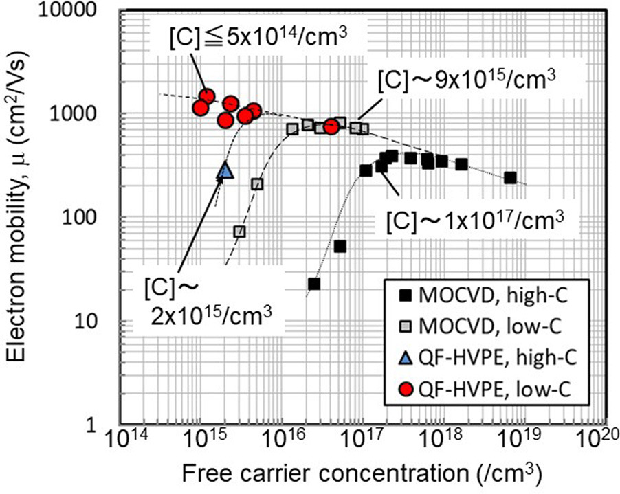
Figure 1: Free-electron density versus mobility in n-GaN layers grown by MOCVD and QF-HVPE with ‘low’ and ‘high’ [C]. MOCVD data from samples grown on sapphire at North Carolina State University et al, and reported in 2016.
The free-carrier density threshold for mobility collapse in MOCVD has been found to be around 2-3x [C]: 3x10¹⁷/cm3 with [C] at 1x10¹⁷/cm3, and 2x10¹⁶/cm3 for 9x10¹⁵/cm3 [C].
The highest mobility of 1470cm2/V-s in the low-[C] QF-HVPE process was found with the free electron density at a very low value of 1.2x10¹⁵/cm3. The researchers comment: “This is the highest reported room-temperature mobility for GaN crystals thus far.”
By introducing a small piece of carbon into the QF-HVPE chamber, the [C} level rose to 2x10¹⁵/cm3. A layer with [Si} at 4x10¹⁵/cm3 saw the free-carrier density drop to 2x10¹⁵/cm3. The mobility was a paltry 288cm2/V-s.
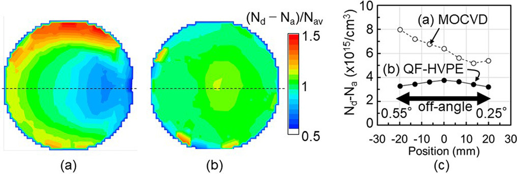
Figure 2: Net carrier concentrations over 2-inch wafers grown by (a) MOCVD and (b) QF-HVPE, according to contactless capacitance-voltage measurements. (c) Line profiles of carrier concentrations along horizontal broken lines in (a) and (b).
The team also measured carrier density uniformity across wafers grown by MOCVD and QF-HVPE (Figure 2). The average carrier densities were 7x10¹⁵/cm3 and 3.4x10¹⁵/cm3, respectively.
The carrier density non-uniformity in the MOCVD had a standard deviation of 16.7%. The researchers comment: “This large variation can be attributed to the off-angle-dependent C-incorporation efficiency, as reported previously.” For the QF-HVPE, the non-uniformity/standard deviation was 4.0% of the already low average carrier density.
Photoluminescence study of the QF-HVPE n-GaN showed sharp 363nm-wavelength near-band-edge emission peak, along with weak broad green emissions centered around 520-530nm. Such green luminescence is associated with nitrogen vacancies. There was no sign of yellow luminescence that is usually attributed to C contamination.
SCIOCS emerged out of Hitachi Cable, and then was part of Hitachi Metals, but is now part of the Sumitomo Chemicals Group. The company is located in the city of Hitachi, where the first company of the same name was founded in 1910.
GaN power devices GaN MOCVD HVPE
https://doi.org/10.1063/5.0014528
https://www.sciocs.com/english/
The author Mike Cooke is a freelance technology journalist who has worked in the semiconductor and advanced technology sectors since 1997.


