


News: Microelectronics
23 April 2020
Dual-layer silicon nitride for threshold engineering gallium nitride transistors
Researchers from China, USA and Canada have used two silicon nitride (SiNx) layers on gallium nitride (GaN) high-electron-mobility transistors (HEMTs) to push the threshold 1V in the positive direction, while reducing off-state leakage and maintaining on-current [Wei-Chih Cheng et al, Semicond. Sci. Technol., vol35, p045010, 2020]. The dual-layer SiNx acts as a stressor, depleting the two-dimensional electron gas (2-DEG) channel under the gate, and as passivation to reduce off-state leakage through the aluminium gallium nitride (AlGaN) barrier layer.
GaN HEMTs are being developed for high-voltage, high-density, high-frequency power switching and radio-frequency (RF) wireless transmission amplification. Although the presented devices were all normally-on (depletion-mode), more positive threshold voltages could eventually lead to normally-off (enhancement-mode) transistors, which reduce power consumption and allow fail-safe high-voltage operation.
The team involved researchers from Southern University of Science and Technology (SUSTech) in China, Hong Kong University of Science and Technology (HKUST) in Hong Kong, China, Washington State University in the USA, University of British Columbia in Canada, GaN Device Engineering Technology Research Center of Guangdong in China, and Key Laboratory of the Third Generation Semi-conductor in China.
The researchers comment: “This Vth increase without recess etching processes or any observable compromises of the gate leakage, DC and RF amplification performance supports strain engineering as an effective approach in pursuing enhancement-mode AlGaN/GaN HEMTs for RF applications.”
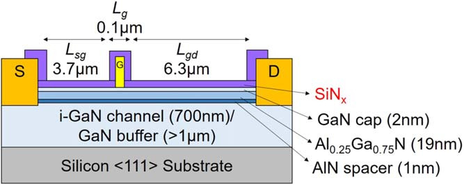
Figure 1: Device structure of AlGaN/GaN HEMT showing gate (Lg), source-to-gate (Lsg), and gate-to-drain (Lgd) lengths/spacings. Channel consisted of unintentionally doped GaN (i-GaN).
The epitaxial material used for the transistors was grown by metal-organic chemical vapor deposition (MOCVD) on 6-inch-diameter <111> silicon at Enkris Semiconductor. The devices (Figure 1) were electrically isolated using inductively couple plasma mesa etching. Annealed titanium/aluminium/titanium/gold formed the ohmic source-drain contacts. The gate consisted of patterned nickel/gold.
The two layers of silicon nitride (SiNx) were deposited using dual-frequency plasma-enhanced chemical vapor deposition (PECVD). The low-stress passivation layer has an unintentional tensile stress of 0.3GPa. The layer used a process avoiding the low-frequency plasma excitation step, to reduce surface damage from nitrogen ion bombardment. The addition of low-frequency plasma excitation for the second layer produced a high-compressive-stress -1GPa film.
The presence of 200nm stressed SiNx enabled the threshold voltage (Vth) to be pushed 1V in the positive direction. Combining the stressor with a 14nm passivation layer increased the on-current to the level of a baseline (BSL) device, which had a 200nm SiNx passivation layer without stressor.
Simulations suggested that the increased threshold derived from electron depletion under the gate caused by the applied compressive stress counteracting the piezoelectric effects of the AlGaN barrier. The tensile stress of the passivation layer only added a negligible amount of electron accumulation, according to the model.
The combined 200nm/14nm stressor/passivation transistor achieved a maximum on-current of 1A/mm (Figure 2). The peak transconductance was 280mS/mm with 7V drain bias, putting the device in the saturation region. The drain current was comparable with the BSL transistor, while the transconductance was higher by around 30mS/mm.
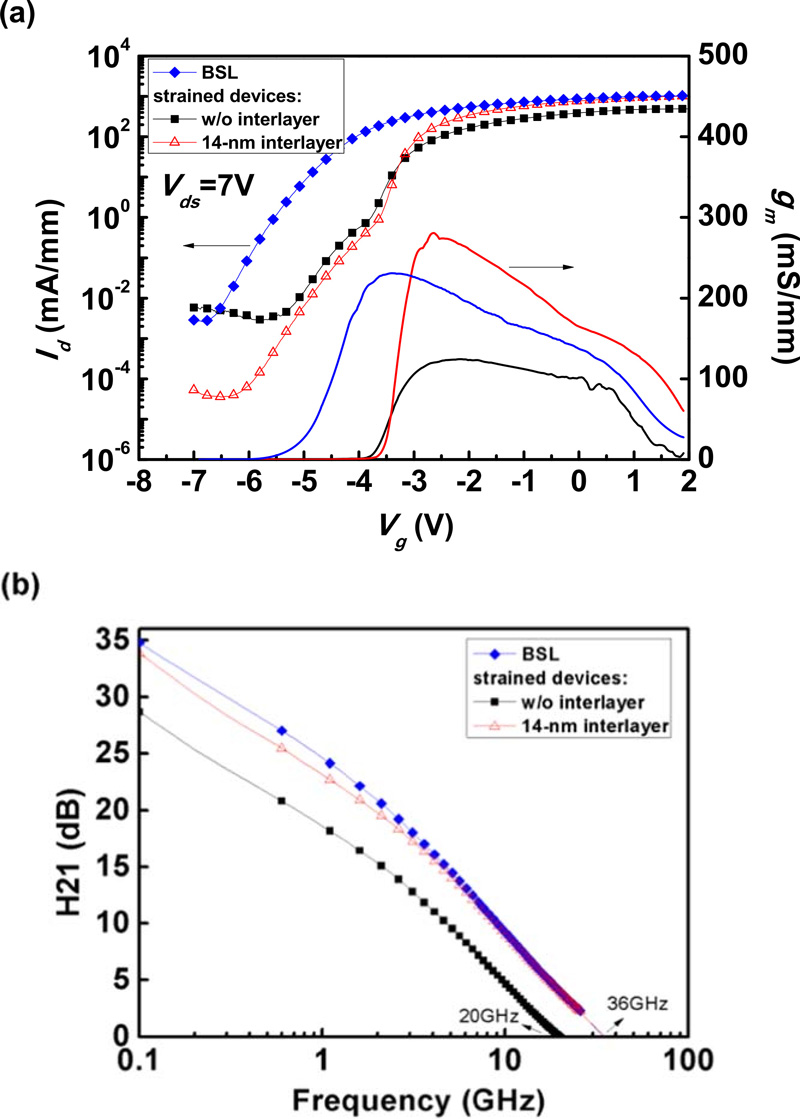
Figure 2: (a) Transfer characteristics of BSL and strained devices at 7V drain bias. (b) H21 current gain of BSL and strained devices biased to 7V drain and 1V above gate threshold.
RF measurements gave a cut-off (fT) of 36GHz, while the stressed device without passivation only achieved 20GHz. The BSL component had a comparable fT of around 36GHz.
The researchers attribute the good performance of the combined stressor/passivation HEMT process to the avoidance of surface damage in the first PECVD step. Surface damage also adversely affected the off-current (Ioff) in the stressed devices without passivation. Adding passivation thicker than 7nm reduced the off-current leakage even below that of the BSL device.
The team summarizes: “From the above data, the devices with 14nm interlayers had the best performance (comparable DC and RF amplification performance, one to three orders of magnitude lower Ioff and 1V higher Vth compared with the baseline devices).”
The researchers also produced micron-scale devices, with 2μm gate and 10μm gate-drain, that were expected to have less effective stressing, which was confirmed by the performance being similar with respect to the BSL architecture in terms of off-current leakage.
GaN GaN HEMTs HEMTs AlGaN MOCVD
https://doi.org/10.1088/1361-6641/ab73ea
The author Mike Cooke is a freelance technology journalist who has worked in the semiconductor and advanced technology sectors since 1997.


